
Passe Passe FPGA Network Switch Example Design
1. Introduction
In this post we will be exploring what it takes to deploy the Passe Passe network switch on a FPGA and measure it’s performance in comparison to an off the shelf dedicated network switch. The example design for this exercise can be found on Github.
2. Project Overview
For this project we will be using a Genesys ZU development board which contains a Zynq Ultrascale+ MPSoC FPGA, part number XCZU3EG-SFVC784-1-E. For the Ethernet ports we will be using a The Quad-port Gigabit Ethernet FMC by Ospero. This Ethernet FMC card is not fully compatible with the Genesys ZU development board but with some clever constraints its possible to make it work although performance will be better with a compatible board. More on this topic at the end.
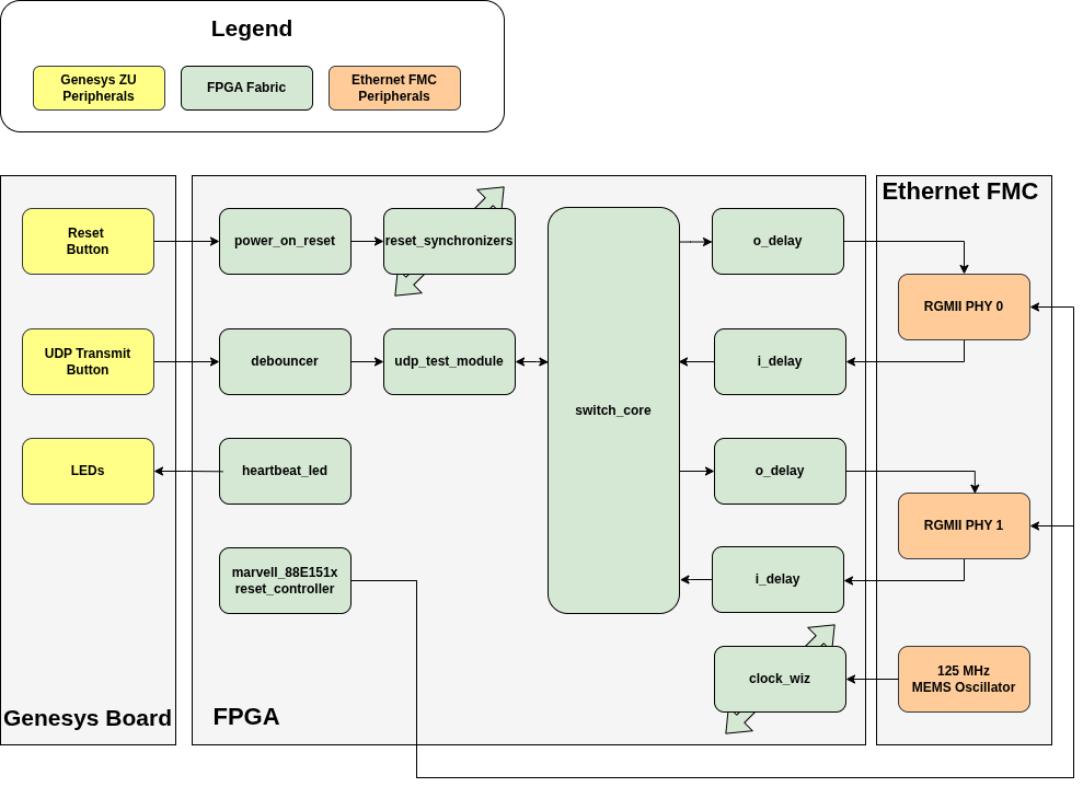
3. Block Diagram
A simplified high level block diagram of the design is shown below.
4. Design Summary
Module level resets are done using an asynchronous power on reset is created using the Xilinx “proc_sys_reset” IP. The IP also takes an external user reset tied to a button on the Genesys board allowing the user to manually reset at any time. The asynchronous reset is then synchronized to the various clock domains using the “reset_synchronizer” module and the synchronized resets are fanned out to the correct locations.
To test the UDP virtual port, a “udp_test_module” is included. This module will send data to the virtual port which will result in an ethernet packet being made and routed by the switch_core to the two RGMII ethernet ports. To trigger this event a button the board is tied to a debouncer module and the deboucned output is connected to the “udp_test_module” as a trigger.
A counter heartbeat module is included to flash the LED, indicating that the board design is running.
The RGMII ethernet PHYs on the Ethernet FMC card are Marvell 88E151x parts and they require a specific timed eset scheme to properly reset the part as described by Section 4.8.1 of the datasheet. To satisfy this reset requirement, the “marvell_88E151x_reset_controller” module creates the reset signal that is supplied to the PHYs.
The switch_core is configured for two RGMII ports and one virtual port.
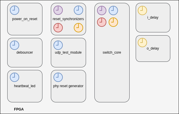
There are several clocks used in this design. A summary of the clocking scheme is shown in the diagrams below.
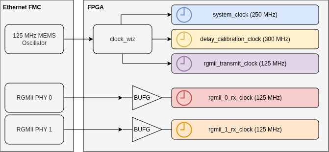
Passe Passe supports various transmit clock schemes for the rgmii_port module. Since this design is intended to only operate in gigabit mode and the PHY will the creating the 2ns delay (90 degree phase shift) for us, we will be supplying our own 125 MHz RGMII transmit clock for best performance.
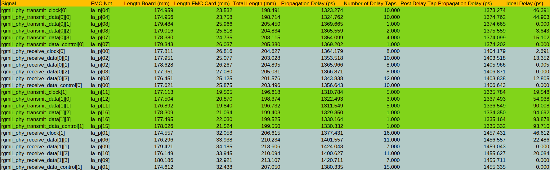
Since we are using an off the shelf development board and FMC card, the trace lengths from the FPGA to the ethernet phys are not matched at all. In order to mitigate this we can use the ODELAY and IDELAY Xilinx IP to create delays. Fortunately, both Digilent and Ospero provide the trace lengths so it is just a matter of putting all the data together. Below is a table summary of the delays for port 0 and port 1. The the table assumes a Tap Delay Step of 5ps and a signal Prorogation Speed of 0.15 mm/ps. The Tap Delay Step size can vary so its best to use time based delay feature of the ODELAY and IDELAY IP. In time mode the IP will calibrate itself and automatically pick the required number of delay taps for the user requested delay.
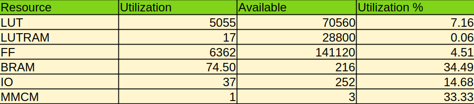
5. Utilization and Power
Overall the utilization and power budget requirements of this design are quite low. The results below are for the example design as configured for two RGMII ports and a single UDP Virtual Port. The largest driver of utilization is the block ram. Passe Passe is not a “cut through” design and instead employs a “buffer and forward” architecture witch CRC checks. A commercial off the shelf “buffer and forward” network switch like the TP-Link TL-SG108-M2 (which we will be benchmarking this design against) has a packet buffer memory size of 1.5 Mb. To implement packet buffers, Passe Passe uses block RAMs. Packet buffer size can be configured depending on how the FIFOs are sized via parameters. You can increase or decrease them for your application. Typically more is better as long as the budget allows it. In this example design each RGMII port has about a 1.5 Mb packet buffer.
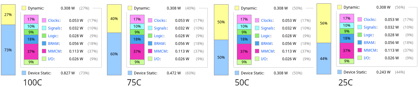
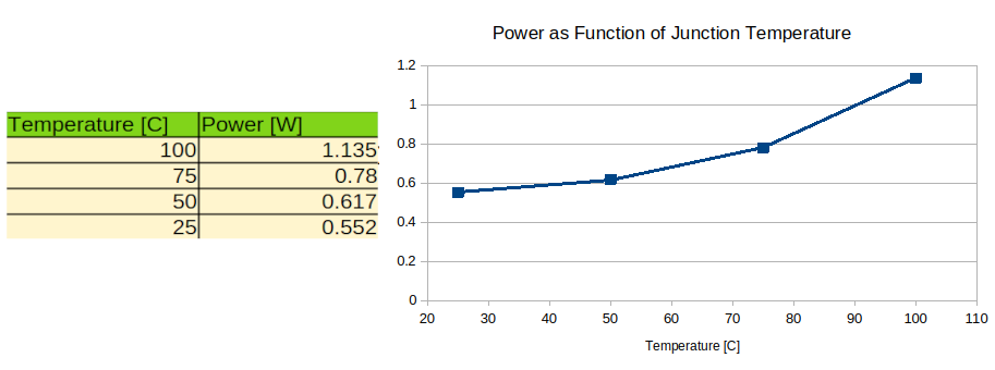
Power is calculated across several junction temperatures below using the Vivado power tool with a liberal toggle rate of 35%. We can see the design is very low power when targeting the XCZU3EG-SFVC784-1-E
6. Creating the Project
To create and build the project as tested, clone the project from the Github report (LINK). Make sure to clone the submodules as well by doing a git submodule update --init –recursive.
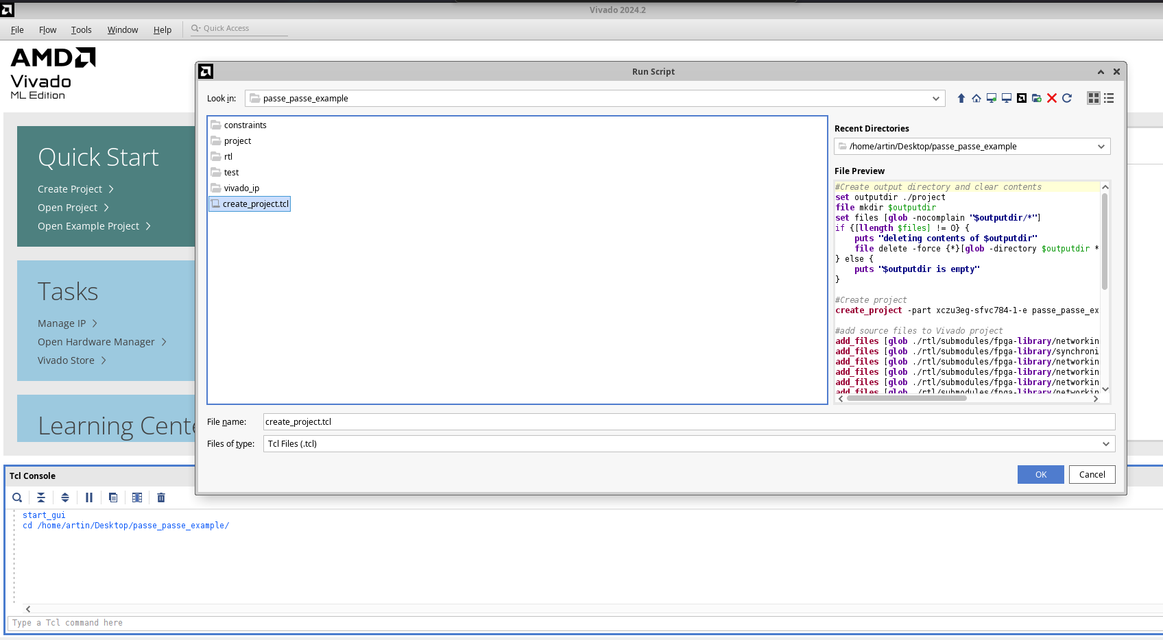
Open Vivado 2024.2, Navigate to to the bottom of the window where the “Tcl Console” is located. Using the console, change the directory to the root directory of the cloned project. Next click Tools in the toolbar header and from the Tools menu click “Run Tcl Script.” From there you can select the “create_project.tcl” file in the root of the cloned repository folder and click OK. This will automatically generate and open the Vivado project.
Before building, open rgmii_port.sv and modify the parameter override on line 313 to change the buffer size. The value used for this test was 131072.
7. Test Setup
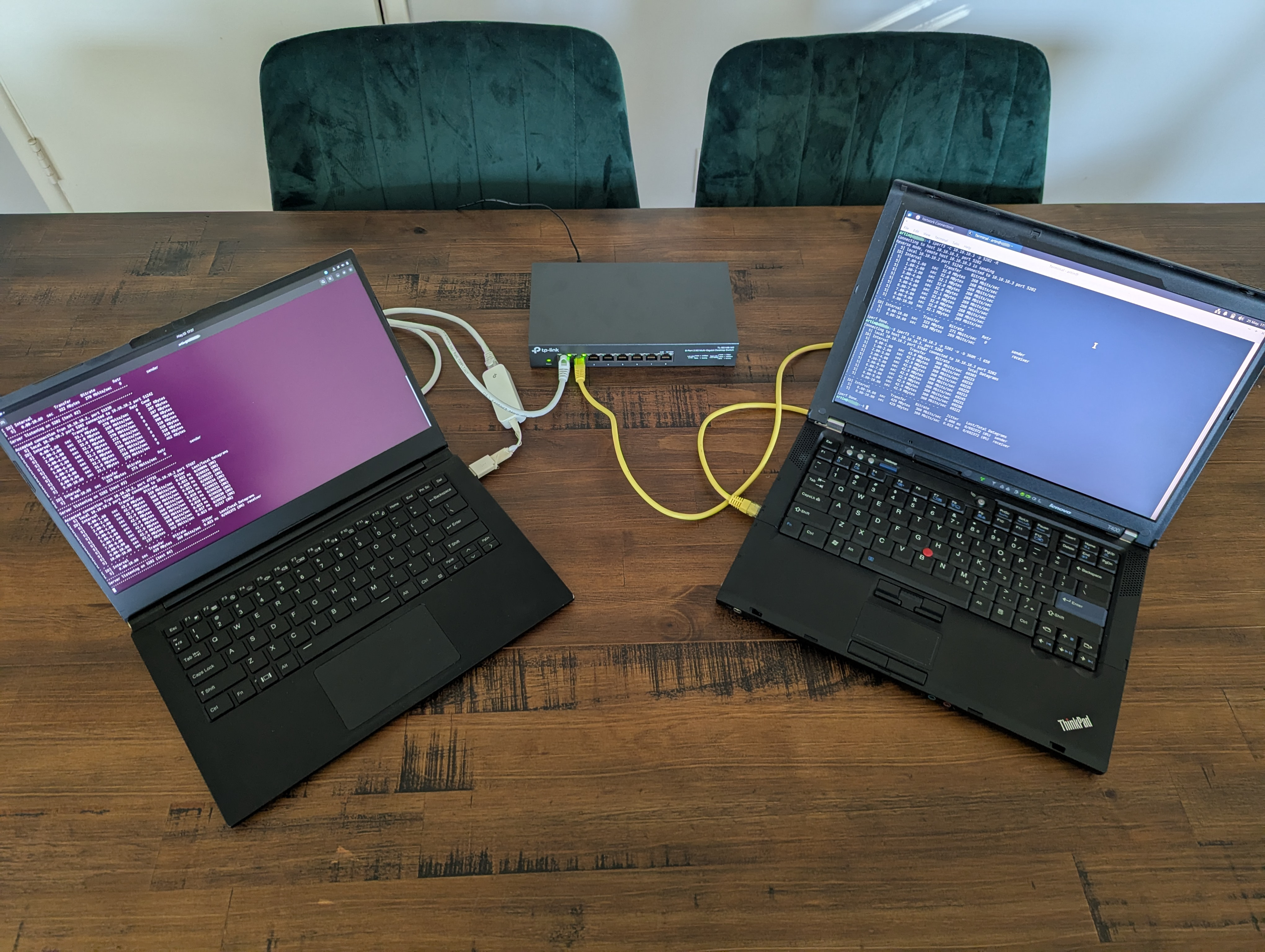
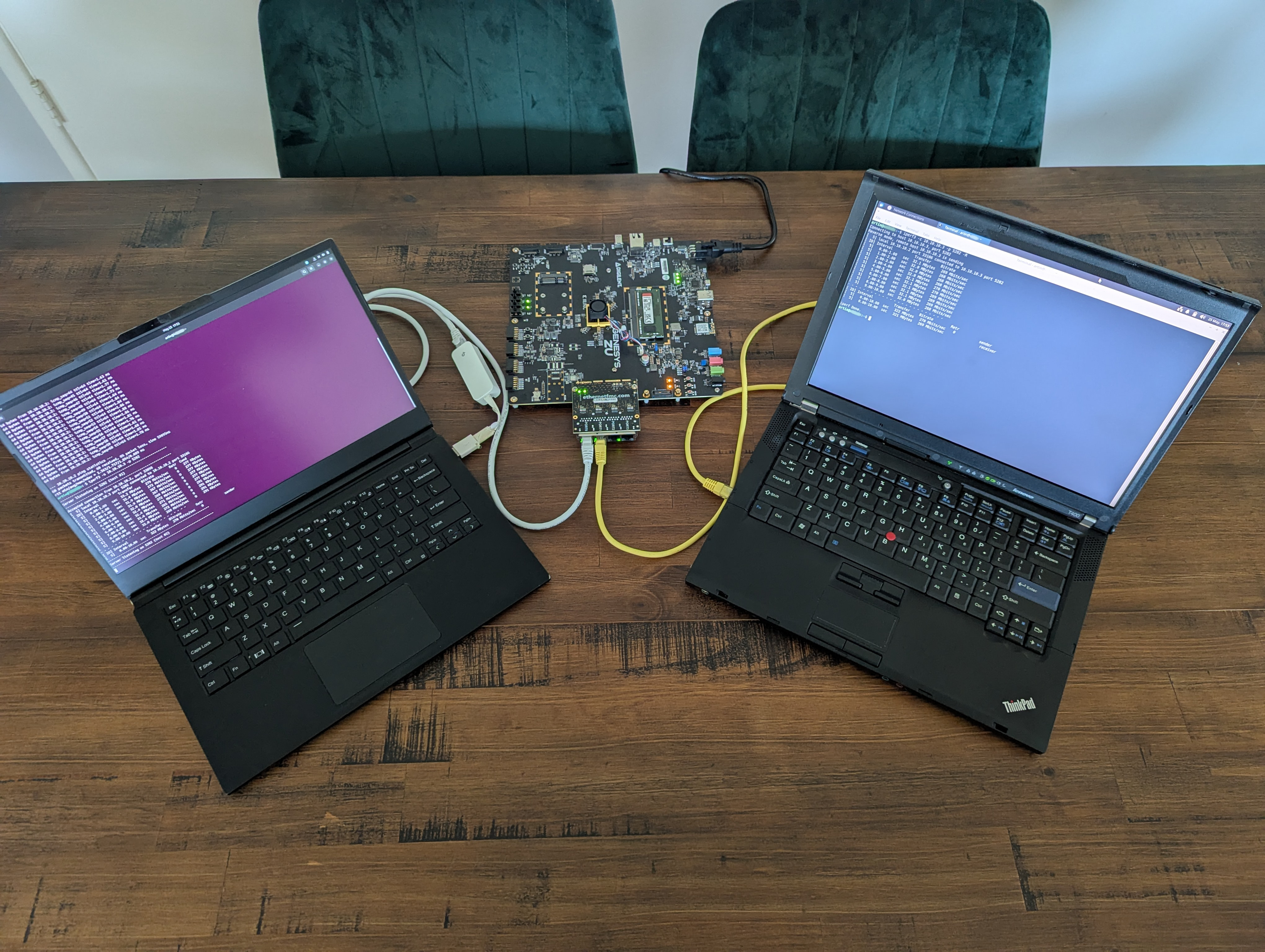
To test the Passe Passe network switch implementation we will use a normal network setup with two personal computers connected to each other through an off the shelf network switch. This setup will serve as the baseline. Then we will replace the commercial switch with Passe Passe and compare the performance. It’s difficult to gauge the performance of the switch by just doing regular web browsing because the performance of the ISP and remote web servers are inconsistent between runs. Therefore, performance will be evaluated using IPerf3 in TCP mode, IPerf3 in UDP mode and with network ping tests. All regular networking services like NTP and ARP are left on and running in the background to more accurately simulate a real world environment. Below is a list of hardware used for each test setup.
| Name | Baseline Setup | Passe Passe Setup |
|---|---|---|
| System 76 Lemur Pro | Yes | Yes |
| TP-Link USB C to Ethernet Adapter (UE300C) | Yes | Yes |
| Lenovo Thinkpad T400 | Yes | Yes |
| TP-Link TL-SG108-M2 | Yes | No |
| Genesys ZU 3EG Development Board | No | Yes |
| Ospero Ethernet FMC 1V8 | No | Yes |
8. Experiment Results
| Experiment | Baseline Result | Passe Passe Result |
|---|---|---|
| IPerf3 Max Error Free UDP Speed | 360 Mbit/sec | 360 Mbit/sec |
| IPerf3 Min Error Free UDP Jitter | 0.020 ms | 0.021 ms |
| IPerf3 Max Error Free TCP Speed | 270 Mbits/sec | 272 Mbits/sec |
| 60 Second Ping Drops | 0 | 0 |
| 60 Second Ping Min | 1.521 ms | 1.531 ms |
| 60 Second Ping Average | 1.735 ms | 1.665 ms |
| 60 Second Ping Max | 3.181 ms | 1.851 ms |
| 60 Second Ping Standard Deviation | 0.228 ms | 0.075 ms |
9. Conclusions and Path Forward
The testing results show that Passe Passe performs equally to the baseline commercial switch. Both setups achieved identical error free UDP speed results while the Passe Passe setup marginally beats the baseline setup in TCP speeds and ping latency results. To push both network switches further and see what their absolute maximum speeds are we will need to setup a new experiment with better equipment, preferably dedicated network switch testing equipment. In the future we will revisit this experiment once more capable computers, NICs, and/or dedicated testing equipment are sourced.
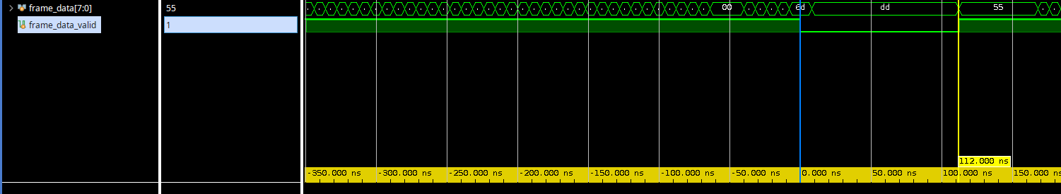
In simulation we can see the overall ingress to outgress latency of the Passe Passe design with a core clock of 250 MHz (as hardware tested) is capable of near gigabit speeds. We can quantify this by seeing what the packet to packet gap is in a simulation test case where packets are continuously fed into one port and routed out the other port. In the example design this is labeled as unit test case_003.
We can see from the screenshot below the minimum inter-packet gap the design always achieves with a core clock of 250MHz is 112ns. 96ns is the standardized absolute minimum required inter-packet for gigabit Ethernet. Therefore at 112ns we should be to achieve near gigabit speeds with the proper test equipment. Furthermore the core clock can be increased past 250MHz to achieve the absolute minimum of 96ns.
To push the Passe Passe HDL implementation even further it will also be very beneficial to replace the Genesys ZU development board with a board that is fully compatible with Ethernet FMC card. Or better yet, building a fully custom PCB with a better speed grade FPGA. The reason the Genesys ZU board is incompatible with the Ethernet FMC card is because only the RX clock on Port 0 is connected to a clock capable pin. To get Port 1 to work, it required the use of experimentally found optimal input delay constraints, locking the clock region of Port 1’s RX clocked logic to X1Y1 (this region is the closest to the input of Port 1’s RX clock pin on this part), and forcing the tools to not use a clock dedicated route for Port 1’s RX clock input. All these settings can be found in the example designs constraints file.