RGMII Ethernet Interface With FPGA
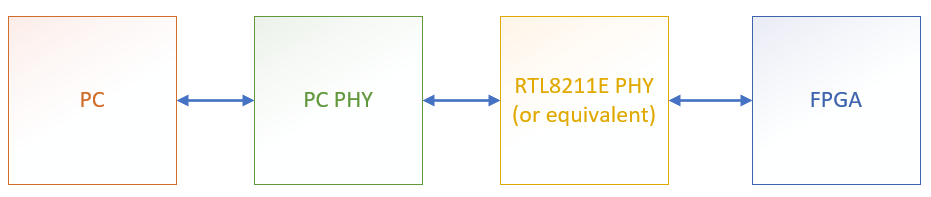
This article is for hardcore digital design wizards who don’t want to use any intermediate processors (kiss your software team goodbye) or proprietary IPs to communicate with their FPGAs via an ethernet connection. All you need is a PC, FPGA, and an ethernet link between them. For this example, we will be using a RT8211E gigabit ethernet PHY on our FPGA side of the link, but any equivalent PHY can work with little to no modification. The RT8211E will be operating with a RGMII (The Reduced Gigabit Media Independent Interface) connection. This is a standardized interface that is supported by many PHYs.
The Github repository containing the latest published version of this design and its corresponding test bench can be found here. The full hardware communication chain can be seen in Figure 1. There are many readily available pieces of software that will enable ethernet communication via your PC however Npcap was used to validate this design. With Npcap this design has been confirmed to operate at full gigabit speeds.
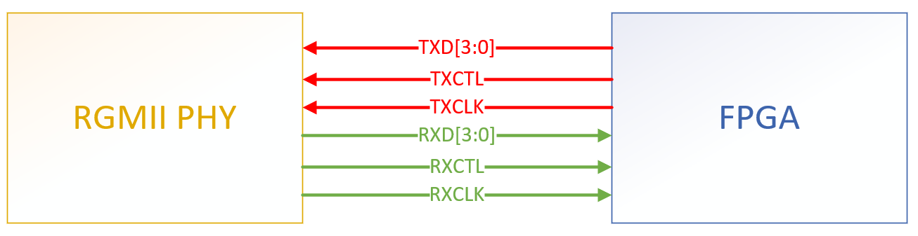
As show in Figure 2 above, both the RX and TX side of this interface contain 6 connections each. 4 data wires (double data rate), one clock wire (125 MHz), and one CTL wire (effectively a data valid signal). The FPGA will be driving or receiving from these wires to communicate with the RGMII PHY.
Ethernet Interface Top
To enable this communication within the FPGA we will be using a series of Verilog modules and block rams wrapped together nicely in a top-level Verilog wrapper. The top-level wrapper is designed to take control signals from and external state machine and execute TX transactions or retrieve RX data. The idea behind this wrapper is to enable the user to integrate this functionality into any potential design. However, all modules including the LFSR generator are standalone units and can be operated independently.
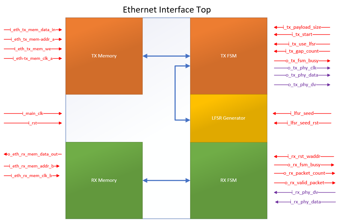
As seen in Figure 3 above, the Ethernet Interface Top module houses the RX memory block ram, RX FSM, TX memory block ram, TX FSM, and the LFSR Generator. The TX memory is a dual port block ram that is written to by an external state machine. The TX FSM pulls data from this TX memory and transmits it to the receiving RGMII transceiver. Alternatively, data can be pulled from the LFSR generator instead. The LFSR generator generates a pseudo random test sequence that can be used to test the transceiver link. The LFSR generator is inverse XOR based so the seed value can be zero. This is useful since most modern popular FPGAs initiate their flip flops with the low (zero) state.
The RX memory is a dual port block ram that can be read via an external state machine and is written to by the RX FSM. If the RX FSM receives a valid ethernet packet, the payload contents of that packet are written to the RX memory. Data from each packet is aligned every 1024 bytes within the RX memory. This means in the presented implementation, payloads should not be greater than 1024 bytes.
All inputs and outs colored RED in Figure 3 are to be interfaced with an external control module. The inputs and outputs colored in PURPLE are to the RGMII transceiver. The only exception to this is "i_main_clk" which should be the 125MHz clock supplied by the PHY. Below we have a detailed port description of the Ethernet Interface Top module.
| Name | Type | Width | Direction | Description |
|---|---|---|---|---|
| i_main_clk | wire | 1 | input | 125MHz clock from PHY. |
| i_rst | wire | 1 | input | Active high synchronous reset. |
| i_tx_payload_size | wire | 16 | input | Number of payload bytes to send via TX FSM. |
| i_tx_start | wire | 1 | input | Active high flag to start TX transmission. |
| i_tx_use_lfsr | wire | 1 | input | Active high flagh to use LFSR data for TX transmission. |
| i_tx_gap_count | wire | 8 | input | Number of gap bytes to transmit after TX packet has beeen sent. |
| o_tx_fsm_busy | wire | 1 | output | Active high TX FSM busy flag. |
| o_tx_phy_clk | wire | 1 | output | TX DDR CLK sent to PHY. This clock is 90 degrees phase shifted version of supplied 125MHz clock. |
| o_tx_phy_data | wire | 4 | output | TX DDR Data sent to PHY. |
| o_tx_phy_dv | wire | 1 | output | TXCTL signal to PHY. Equivalent to a data valid signal. |
| i_rx_rst_waddr | wire | 1 | input | Active high flag to reset write address pointer used by RX FSM. |
| o_rx_fsm_busy | wire | 1 | output | Active high RX FSM busy flag. |
| o_rx_packet_count | wire | 10 | output | RX DDR Data recieved from PHY. |
| o_rx_valid_packet | wire | 1 | output | Active high pulse indicating a new valid packet has been captured. |
| i_rx_phy_dv | wire | 1 | input | RX RXCTL signal from PHY. Equivalent to a data valid signal. |
| i_rx_phy_data | wire | 4 | input | RX DDR Data recieved from PHY. |
| i_lfsr_seed | wire | 32 | input | Seed value used by LFSR generator. |
| i_lfsr_seed_rst | wire | 1 | input | Active high reset LFSR generator seed. |
| i_eth_tx_mem_data_in | wire | 8 | input | Data write port of block ram read by TX FSM. (Port A) |
| i_eth_tx_mem_addr_a | wire | 16 | input | Data writeaddress port of block ram read by TX FSM. (Port A) |
| i_eth_tx_mem_we | wire | 1 | input | Data write enable port of block ram set by TX FSM. (Port A) |
| i_eth_tx_mem_clk_a | wire | 1 | input | TX Mem Clk (Port A) |
| o_eth_rx_mem_data_out | wire | 8 | output | Data out port of black ram filled by RX FSM (Port B) |
| i_eth_rx_mem_addr_b | wire | 16 | input | Data read address of block ram filled by RX FSM (Port B) |
| i_eth_rx_mem_clk_b | wire | 1 | input | RX Mem Clk (Port B) |
ETH TX FSM
The ETH TX FSM transmits data to the receiving RGMII PHY. Data is pulled in from either the TX memory or the LFSR generator. If the busy flag (o_busy) is low, the TX FSM will begin transmitting data if the i_eth_tx_start input is high. After the packet is sent, the state machine will wait "i_gap_count" clock cycles before being able to transmit again. This allows to user to program in some dead time between transmits. Once done transmitting the o_busy output flag will go low again. If LFSR data is to be used, the "i_lfsr_data" input must be set high.
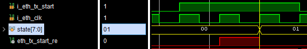
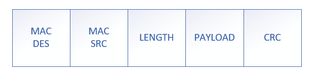
The state machine takes in the 125MHz clock provided by the PHY however the output data clock, "o_eth_txck" is a 90 degrees phase shifted version of i_clk. This gives us 2ns of data setup time satisfying the 1.8ns of setup time required by most RGMII PHYs. To generate this clock a PLL/MMCM is used and the resulting waveforms should look similar to what is seen in Figure 6. The transmitted data itself is a full ethernet packet consisting of the seven sections shown in Figure 5. The state machine has a state for each portion of the packet structure shown in Figure 5.
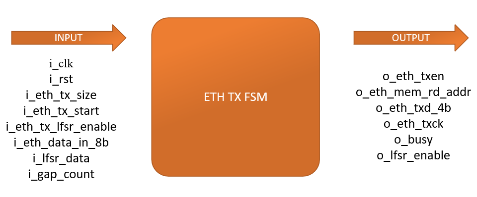


| Name | Type | Width | Direction | Description |
|---|---|---|---|---|
| i_eth_clk | wire | 1 | input | 125MHz clock from PHY. |
| i_rst | wire | 1 | input | Active high synchronous reset. |
| i_eth_tx_size | wire | 16 | input | Number of payload bytes to send. |
| i_eth_tx_start | wire | 1 | input | Active high flag to start TX transmission. |
| i_eth_tx_lfsr_enable | wire | 1 | input | Active high flag to use LFSR sequence as data. |
| i_eth_data_in_8b | wire | 8 | input | Data pulled from TX memory. |
| i_lfsr_data | wire | 8 | input | LFSR data pulled from LFSR generator. |
| i_gap_count | wire | 8 | input | Number of gap bytes to transmit after TX packet has been sent. |
| o_eth_txen | wire | 1 | output | TXCTL signal to PHY. Equivalent to a data valid signal.. |
| o_eth_mem_rd_addr | reg | 16 | output | Read address to TX Memory. |
| o_eth_txd_4b | wire | 4 | output | TX DDR Data sent to PHY. |
| o_eth_txck | wire | 1 | output | TX DDR CLK sent to PHY. This clock is 90 degress phase shifted version of the supplised 125 MHz clock. |
| o_busy | reg | 1 | output | Active high flag indicating FSM is busy transmitting. |
| o_lfsr_enable | reg | 1 | output | Active high flag to enable LFSR generator. |
Detailed TX FSM State Machine Flow
Below we will be going over each state presented in the TX FSM state machine flow graph shown in Figure 7.
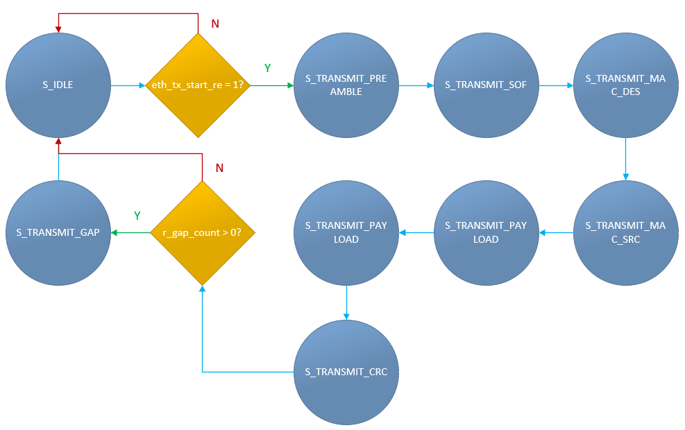
1. S_IDLE (8’h00)
If positive edge of i_eth_tx_start is detected, cache i_tx_size, i_gap_count, i_eth_tx_lfsr_enable, i_mac_destination, i_mac_source, and begin transmission of data.
2. S_TRANSMIT_PREAMBLE (8’h01)
Transmit seven bytes of preamble character (0x55)
![]()
3. S_TRANSMIT_SOF (8’h02)
Transmit one start of frame character (0xD5). Enable CRC32 calculation as well. The CRC32 of the destination, source, and payload bytes must be calculated which will be transmitted next.
![]()
3. S_TRANSMIT_MAC_DES (8’h03)
Transmit the 48bit mac destination, MSB first.
![]()
4. S_TRANSMIT_MAC_SRC (8’h04)
Transmit the 48bit mac source, MSB first.
![]()
5. S_TRANSMIT_PAYLOAD (8’h05)
Transmit data received from outbuffer (i_eth_data_in_8b). Increment outbuffer address (o_eth_mem_rd_addr) until it is less than or equal to tx_size. Disable CRC32 calculation. This will cause the CRC32 module to start outputting CRC32 values.
![]()
6. S_TRANSMIT_CRC (8’h06)
Transmit the four CRC32 bytes outputted from the CRC32 module. If gap_count is zero, return to S_IDLE.
![]()
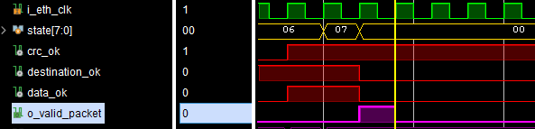
7. S_TRANSMIT_GAP (8’h07)
Wait r_gap_count clock cycles before returning to idle.
![]()
ETH RX FSM
The ETH RX FSM receives data from the ethernet PHY. The RX FSM scans for a packet with the correct mac source, mac destination, and CRC32. This data is written to the RX Memory and if the data is valid the “o_valid_packet “output pulses high. The address pointer to the RX memory is 1024 byte aligned and can be reset if i_eth_rst_waddr is set high while the FSM is not busy. The packet counter “o_packet_count” will also be reset. The address pointer is set to the next 1024 aligned address if a valid packet is detected. The “o_packet_count” counter is incremented when a valid packet is detected. The "o_busy flag" indicates whether the RX FSM is processing a potentially valid ethernet packet.
The RX FSM will self-calibrate and adjust its data capturing to account for delays in the data line. The received packet should be partitioned as shown in Figure 10. The “length” portion of the packet should be two bytes and will tell the RX FSM how many payload bytes to capture. The state machine does not care about the RXCTL signal, the preamble or start of frame bytes. Since it is always scanning for data, it is irrelevant whether those bytes are processed as the data validity checks will ensure it is receiving an actual ethernet packet. Since we also do not use the RXCTL signal, it is very important that the length bytes are present and accurate as it will tell the state machine when the packet ends. Ignoring the RXCTL signal also eliminates the possibility of delays in that signal line affecting the state machine.
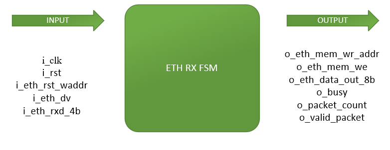
| Name | Type | Width | Direction | Description |
| i_eth_clk | wire | 1 | input | 125MHz clock from PHY |
| i_rst | wire | 1 | input | Active high synchronous reset |
| i_eth_rst_waddr | wire | 1 | input | Active high flag to reset RX mem write address pointer to zero |
| i_eth_dv | wire | 1 | input | RX RXCTL signal from PHY. Equivalent to a data valid signal. |
| i_eth_rxd_4b | wire | 4 | input | RX DDR data recieved from PHY |
| o_eth_mem_wr_addr | reg | 1 | output | RX Memory Write Address |
| o_eth_mem_we | reg | 1 | output | RX Memory Write Enable |
| o_busy | reg | 1 | output | Active high flag indicating FSM is busy transmitting |
| o_packet_count | reg | 10 | output | Number of packets captured by RX FSM into memory |
| o_valid_packet | reg | 1 | output | Active high pulse indicating a new valid packet has been captured |
Detailed RX FSM State Machine Flow
Below we will be going over each state presented in the TX FSM state machine flow graph shown in Figure 9.
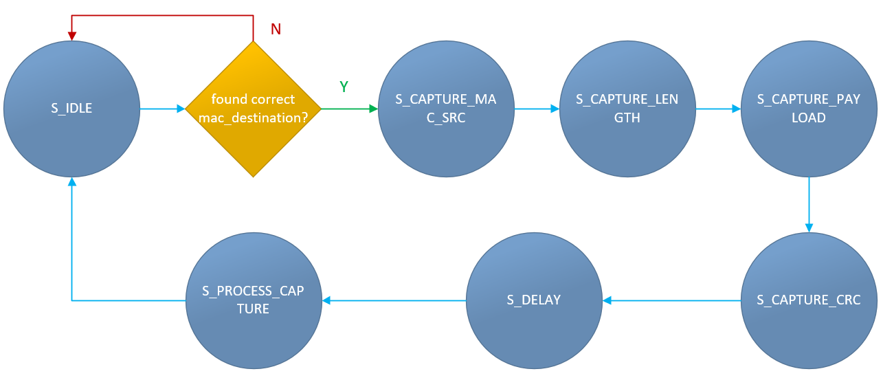
1. S_IDLE (8’h00)
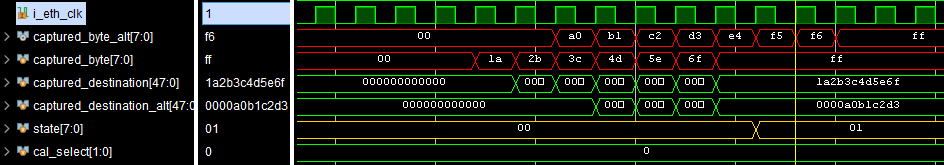
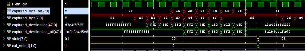
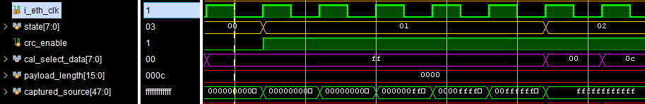
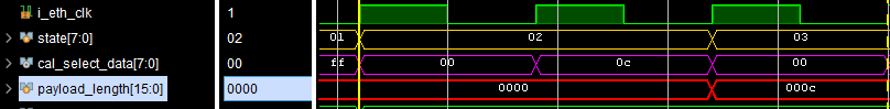
If i_eth_rest_waddr is detected, set RX memory address pointer (o_eth_mem_wr_addr) and packet counter (o_packet_count) to zero. Otherwise continuously scan for the target mac address destination. Since data line delays are not guaranteed, the state machine performs a self calibration in this state by looking for the target mac address for both the normal delay case and extra delay case. If the correct mac address has been detected, the correct delay calibration is selected (cal_select) and all further reads will be parsed using the selected calibration. The CRC32 module is also enabled before proceeding to subsequent states. Below we can see data received with normal delays (Figure 11) and data received with extra delays (Figure 12).
2. S_CAPTURE_MAC_SRC (8’h01)
Capture six bytes of data and shift them into the captured_source register. This 48 bit register contains the mac address source portion of the ethernet packet.
3. S_CAPTURE_LENGTH (8’h02)
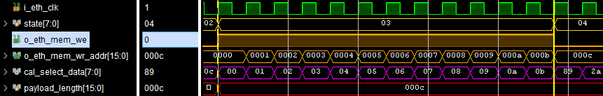
Capture two bytes of data corresponding and store them in the payload_length register. This 16-bit register determines the number payload data bytes are read in the next state. Since we are not using the RXCTL signal, we determine when to stop reading data via this register. We also set the RX memory write enable (o_eth_mem_we) high before proceeding to the next state.
4. S_CAPTURE_PAYLOAD (8’h03)
Capture data and increment the RX memory write address pointer (o_eth_mem_wr_addr) and the counter register. Once the counter register equals the payload_length register, stop writing to RX memory and proceed to capture the CRC32.
5. S_CAPTURE_CRC (8’h04)
Capture four bytes of data corresponding to the CRC32 portion of the ethernet packet.
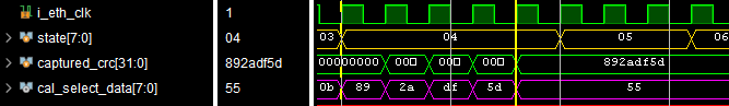
6. S_DELAY (8’h05)
Wait for CRC32 module to process all data, then disable it and wait for it to start returning the computed CRC32. This computed value will be compared with the received value as a data validity check.
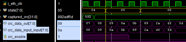
7. S_COMPARE_CRC (8’h06)
Shift in computed CRC32 value into the computed_crc register.
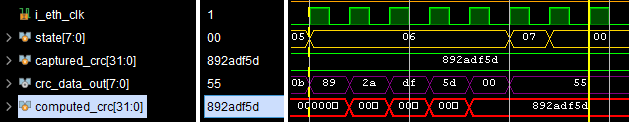
8. S_PROCESS_CAPTURE (8’h07)
If the captured data is valid, pulse the o_valid_packet output high. Increment the packet counter and set the address pointer to the next 1024 aligned address. This alignment organizes the RX memory such that every group of 1024 address contains exactly one received ethernet packet. Data is valid if the computed CRC32 is equal to the captured CRC32 and the captured mac destination equals the target mac destination. We also reset various registers back to zero, including the busy flag, and return to the S_IDLE state.