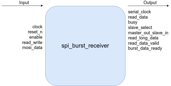
Super SPI Master Verilog Module With Burst Capability
This robust SPI master module allows fully operational SPI reading and writing as well as burst read/write capability. An accompanying burst read capture state machine is provided as well for complete drop in applications into any FPGA project. System Verilog source and test bench can be found on my Github page (direct link here).
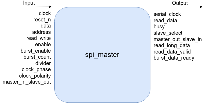
SPI Master Top Level Overview
|
Name |
Type |
Width |
Direction |
Description |
|---|---|---|---|---|
| clock |
wire |
1 |
input |
Main system clock (note: not the actual SPI SCLK) |
| reset_n |
wire |
1 |
input |
Active low reset |
|
data |
wire |
DATA_WIDTH |
input |
Data to be written during data phase of SPI transaction |
|
address |
wire |
ADDRESS_WIDTH |
input |
Address to be written during the address phase of SPI transaction |
|
read_write |
wire |
1 |
input |
read_write = 0 will signify a WRITE request, read_write = 1 will signify a READ request |
|
enable |
wire |
1 |
input |
Active high enable signal that begins a transaction if master is not busy |
|
burst_enable |
wire |
1 |
input |
Active high burst enable signal, if high before a transaction the transaction will be a burst transaction |
| burst_count |
wire |
16 |
input |
Number of burst transactions to execute |
|
divider |
wire |
16 |
input |
Divider value used to calculate the SPI SCLK |
| clock_phase |
wire |
1 |
input |
SPI CPHA config |
|
clock_polarity |
wire |
1 |
input |
SPI CPOL config |
| master_in_slave_out |
wire |
1 |
input |
SPI MISO connection |
|
serial_clock |
logic |
1 |
input |
SPI SCLK connection |
|
read_data |
reg |
DATA_WIDTH |
output |
Data received from slave (half-word) |
| busy |
reg |
1 |
output |
State machine busy flag (active high) |
|
slave_select |
reg |
1 |
output |
SPI SS/CS connection |
|
mast_out_slave_in |
reg |
1 |
output |
SPI MOSI connection |
|
read_long_data |
reg |
DATA_WIDTH+ADDRESS_WIDTH+1 |
output |
Data received from slave (full-word) (latched output) |
|
read_data_valid |
reg |
1 |
output |
Active high pulsed signal indicating wether a new word has been read by the master |
|
burst_data_ready |
reg |
1 |
output |
Active high signal indicating next word for burst write should be fed into the data input |
|
Name |
Typical Value |
|---|---|
|
DATA_WIDTH |
8/16 |
|
ADDRESS_WIDTH |
7/15 |
Clock Divider
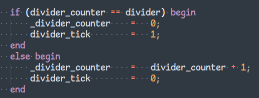
This module is designed to utilize the same system clock as the rest of your design. By doing this we can minimize situations where they could be potential inter clock path timing violations. However, in most cases such clocks are in the megahertz range and running SPI transactions at those rates are unrealistic, therefore we need a mechanism to divide our clock down. To do so we will be using a simple counter-based divider. The “divider_counter” is a 16 bit register that is continuously incremented. When it is equal to the “i_divider” value, our divider tick wire will pulse high, and the counter will return to zero. This divider tick pulse will signal the main state machine to execute an operation. It is important to still drive the main state machine’s flip flops at the system clock and have the divider tick be a gate keeper with an if statement. Although driving the flip flops using the divider register directly as a clock will look fine in simulation, the implemented design will have erratic behavior because FPGAs typically use dedicated optimized paths for clocks that are different from register paths. The SPI SCLK frequency can be calculated using the equation below.
$$f_{SCL} = \frac{f_{CLK}}{4(divider+1)}$$
SPI Master State Machine Overview
This module operates as a finite state machine with a state for each portion of a typical SPI transaction. The FSM defaults to the IDLE state where it waits for the appropriate control signals to execute a read or write SPI transaction. A flow chart for the FSM and a detailed overview of each state is shown below.
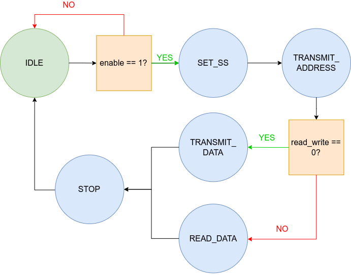
S_IDLE
Saves the following inputs into internal registers: read_write, clock_phase, clock_polarity, burst_count, address, data. These stored values will be used throughout the transaction.
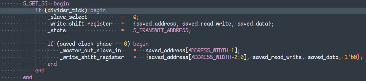
S_SET_SS
Sets slave select slave select low. If CPHA = 0, it is important to shift the first bit of our message out during the this state before going to the S_TRANSMIT_ADDR state to meet setup time requirements.
S_TRANSMIT_ADDRESS
Shift out the address of the SPI register we will be reading/writing to. This address includes the actual “read_write” bit which will tell the slave whether we want to execute a read or a write. Data that is shifted out from the slave is also recorded in this state and will be available in the "read_long_data" output.
S_TRANSMIT_DATA
If a write was requested the master will begin shifting out the data to be written to the address during this state. Again, all data that is shifted out from the slave is still recorded during this state.
If in burst mode, the state machine will loop through this state until it has done writes equal to the value stored in the “burst_num” register. When shifting out the last bit of the current data to be written, the o_burst_write_word_request flag of the state machine will go high. When this condition occurs, new data should be supplied to the i_data input. The state machine will store this when "process_counter" == 2 and will write this new data during the next iteration of the burst write sequence. This scheme allows an external state machine ¼ SCLK period in order to latch in new words to be written during the burst sequence.
S_READ_DATA
If a read was requested the master will read data during this state. Throughout the process, the master will continuously shift out 1’b1 on the MOSI line.
If in burst mode, the state machine will loop through this state until it has done reads equal to the value stored in the “saved_burst_count” register. When the last bit of the current iteration’s word is read the "read_data_valid" output is pulsed high. During this time, the external burst read state machine must process the read data that is stored in the "read_word" output.
S_STOP
Here SS is set high again to end the SPI transaction. If CPHA = 1 the last bit of the word is read when "process_counter" == 0. This is done to meeting SPI timing requirements much like how the first bit is transmitted in the S_IDLE state when CPHA = 0.
SPI Master Recommended Usage
When using this master the "busy" is the cirtical flag to monitor in order to easily keep track of what the master is doing. It is recommend to first set the configruation inputs of the master. This includes "data", "address", "read_write", "burst_count", "clock_phase", "clock_phase" and "divider". Then query the "busy" output signal, once it is low set "enable" (and "burst_enable" if a burst is required) high. Once the "busy" output goes high, we set "enable" (and "burst_enable" if a burst is required) low. Finally once "busy" is low again, we know the transaction has been completed. Each new time the "read_data_valid" output pulses, we have a new word read by the master stored in the "read_data" output. If a burst write is requested, it is important to monitor the "burst_data_ready" output. When it pulses high, a new word must be supplied to the "data" input before "burst_data_ready" signal goes low again other wise it will send whatever word was at the "data" input.
SPI Signal and Timing Requirements
This master is capable of operating in all four available SPI modes. Below are examples of how a master will behave for each of the four possible SPI configuration parameters.
CPHA = 0, CPOL = 0
1. MOSI/MISO setup half SCLK period before RISING edge of SCLK. Data is sampled after the rising edge of SCLK
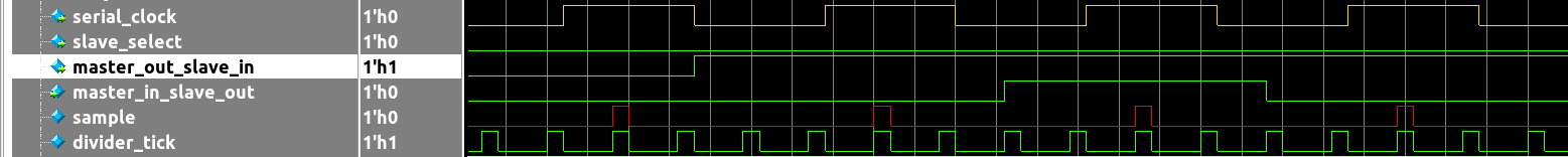
2. SS should be set low half SCLK period before RISING edge of first SCLK pulse

3. SS should be set high half SCLK period after FALLING edge of last SCLK pulse

CPHA = 0, CPOL = 1
1. MOSI/MISO setup half SCLK period before FALLING edge of SCLK. Data is sampled after the FALLING edge of SCLK.
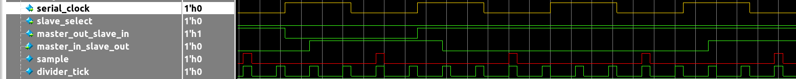
3. SS should be set low half SCLK period before the first falling edge of SCLK

4. SS should be set high half SCLK period after the last RISING edge of SCLK

CPHA = 1, CPOL = 0
1. MOSI/MISO setup half SCLK period before FALLING edge of SCLK. Data is sampled after FALLING edge of SCLK
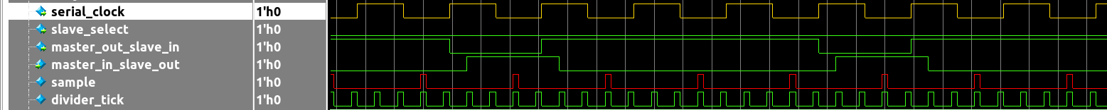
2. SS should be set low half SCLK period before RISING edge of first SCLK pulse

3. SS should be set high half SCLK period after FALLING edge of last SCLK pulse

CPHA = 1, CPOL = 1
1. MOSI/MISO setup half SCLK period before RISING edge of the following SCLK. Data is sampled after RISING edge of SCLK.
2. SS should be set low half SCLK period before FALLING edge of SCLK

3. SS should be set high half SCLK period after last RISING edge of SCLK

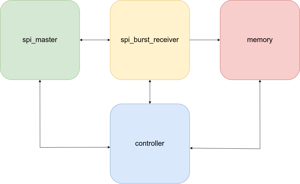
Burst Read Capture FSM Top Level Overview
The burst read capture state machine is a module that is meant to support the SPI master during burst reads. It's purpose is to demonstrate how the master behaves during a burst read transaction and how to effectively store these burst reads into a memory in a timely fashion in order to guarantee all data is captured during a burst read transaction.
|
Name |
Type |
Width |
Direction |
Description |
|---|---|---|---|---|
| clock |
wire |
1 |
input |
Main system clock |
|
reset_n |
wire |
1 |
input |
Active low reset |
| enable | wire | 1 | input | Active high signal to start the capture FSM |
| burst_count |
wire |
16 |
input |
Number of burst reads to process from the SPI Master |
|
burst_data_enable |
wire |
1 |
input |
Pulsed active high signal signifying new SPI data can be processed from SPI Master |
|
burst_data |
wire |
16 |
input |
Read SPI data from SPI Master |
|
busy |
reg |
1 |
output |
State machine busy flag (active high) |
|
data_valid |
reg |
1 |
output |
Active high captured data valid flag |
|
data |
reg |
16 |
output |
Captured data |
|
memory_address |
reg |
16 |
output |
Address write pointer for captured data |
Capture State Machine Overview
This module is a simple state machine with three states that is intended to be used in conjunction with the SPI master state machine. It will wait in the default idle state until it is armed with the start single. Once armed, the state machine will capture read data from the SPI master state machine and write them to an external memory module. A flow chart of the state machine and a detailed overview of each state can be found below.
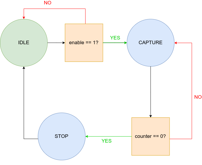
S_IDLE
Waits for "enable" input to be high in order to start capturing burst read data. Stores "burst_count" input into the "counter" register.
S_CAPTURE
Will wait until a positive edge of the "burst_data_enable" input signal is detected. When this condition is met, the read SPI data will be written to memory and a counter will be incremented. This counter is used to keep track of the number of burst read values processed.
S_DONE
After all the burst data is read the "busy" output will transition low and all miscellaneous signals will be reset here before looping back into the S_IDLE state.
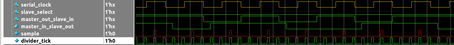
Burst Read Capture Recommended Usage
As mentioned before, this module is meant to be used with conjunction to the SPI Master state machine. Its sole purpose is to offload the burst read data from the SPI Master into a memory. It is recommended to control both the SPI Master module and the Burst Read Capture module with the same external control module. This control module should monitor the outputs and set the inputs of both the master and capture machine. It is important to arm the capture state machine first before starting a burst read operation. Also, it is critical that both the master and read capture state machine have the same value supplied to their respective "burst_count" input. This input tells the master how many reads to execute and tells the capture state machine how many reads to capture. Therefore, it is important for them to match. Below is a recommended block diagram of how the overall system should be laid out as well as a screenshot of the provided test bench where it shows how to use the capture state machine.