
Tiny But Mighty I2C Master Verilog Module
This easy to use System Verilog I2C master module allows easy drop in operation into any FPGA project and allows for effective and reliable I2C master operation. In this post we will be discussing the workings and details of this module. System Verilog source and test bench can be found on my Github page (direct link here).
Top Level Overview
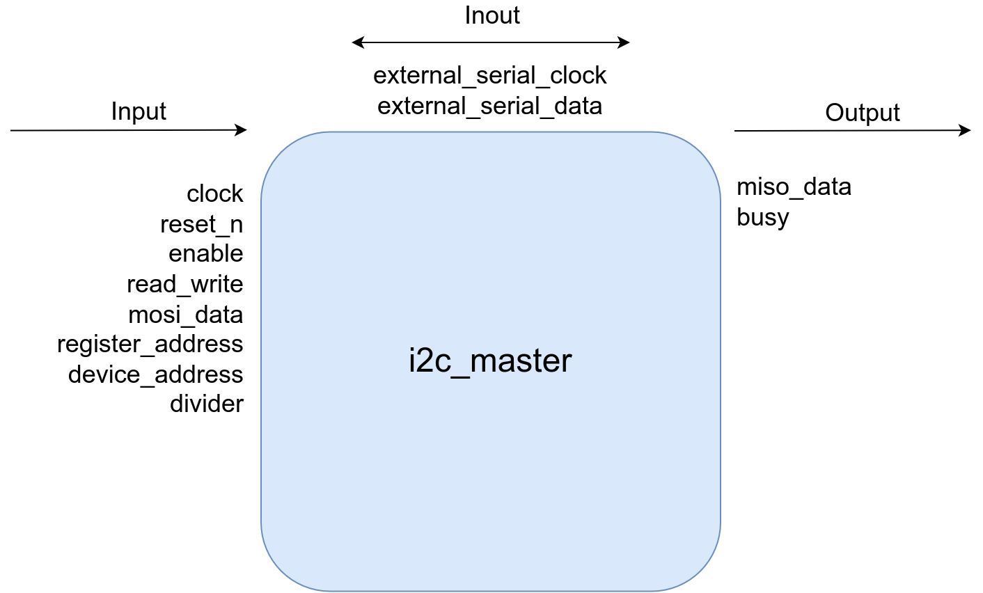
| Name | Type | Width | Direction | Description |
|---|---|---|---|---|
| clock | wire | 1 | input | Main system clock (note: not the actual I2C SCL) |
| reset_n | wire | 1 | input | Active low reset |
| enable | wire | 1 | input | Active high enable signal that begins a transaction if master is not busy |
| read_write | wire | 1 | input | read_write = 0 will signify a WRITE request. read_write = 1 will signify a READ request. |
| mosi_data | wire | NUMBER_OF_DATA_BYTES*8 | input | Data to be written to a register during an I2C write transaction |
| register_address | wire | NUMBER_OF_REGISTER_BYTES*8 | input | Register where data is read/written during an I2C transaction |
| device_address | wire | ADDRESS_WIDTH | input | Target slave address |
| divider | wire | 16 | input | Divider value used to calculate the I2C clock rate. |
| miso_data | reg | NUMBER_OF_DATA_BYTES*8 | output | Data read during a READ operation. |
| busy | reg | 1 | output | When high master is busy with a READ/WRITE transaction. |
| external_serial_data | wire | 1 | inout | SDA conenction for I2C bus |
| external_serial_clock | wire | 1 | inout | SCL connection for I2C bus |
| Name | Description |
|---|---|
| NUMBER_OF_DATA_BYTES | Number of 8 bit words (bytes) to be sent to or read from the slave during the data transaction states. Setting this to a value of 0 will default to a single byte. |
| NUMBER_OF_REGISTER_BYTES | Number of 8 bit words (bytes) to be sent to the slave during the register transaction Setting this to a value of 0 will default to a single byte. |
| CHECK_FOR_CLOCK_STRETCHING | Setting this to a non zero value will enable clock stretching checks by the master. |
| CLOCK_STRETCHING_MAX_COUNT | Number of divider tick pulses to wait while slave is stretching the clock. Lowering this value will effectivley limit the maximum amount of clock stretching a slave can request. |
This module is tested and designed to run in either 8-bit mode or 16-bit mode. In 8-bit mode the data and registers are represented with 8bit numbers while in 16bit mode they are represented with 16bit numbers. The mode can be changed by overriding the DATA_WIDTH and REGISTER_WIDTH parameters. Alternatively a combination of 8-bit and 16-bit data/register widths can be used as well.
State Machine Overview
This module is designed as to operate as a finite state machine. Although there are a number of states we can simplify and represent the state machine as a machine consisting of three states.
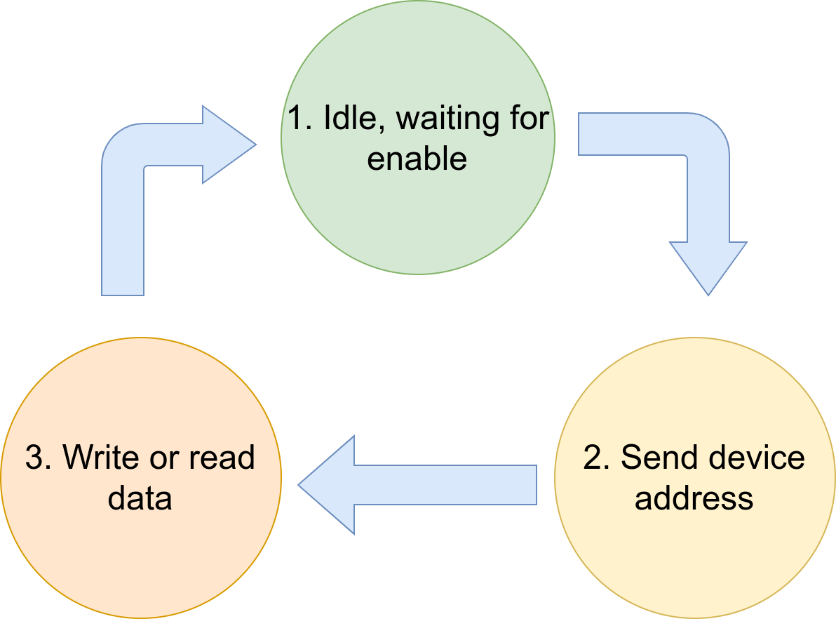
1. Idle - Here the master checks its inputs for a command and executes the read/write command based on its input.
2. Write Device Address - To begin executing the command the master first sends the I2C address of the slave device with the r/w operation bit appended.
3. Write / Read Data - Once the slave acknowledges its address, the reading or writing is executed.
Clock Divider
This module is designed to utilize the same system clock as the rest of your design. By doing this we can minimize situations where they could be potential inter clock path timing violations. However, in most cases such clocks are in the megahertz range and running I2C transactions at those rates are unrealistic, therefore we need a mechanism to divide our clock down. To do so we will be using a simple counter-based divider. The “divider_counter” is a 16 bit register that is continuously incremented. When it is equal to the “divider” input value, our divider tick wire will pulse high, and the counter will return to zero. This divider tick pulse will signal the main state machine to execute an operation. It is important to still drive the main state machine’s flip flops at the system clock and have the divider tick be a gate keeper with an if statement. Although driving the flip flops using the divider register directly as a clock will look fine in simulation, the implemented design will have erratic behavior because FPGAs typically use dedicated optimized paths for clocks that are different from register paths. The I2C SCL frequency can be calculated using the equation below.
$$f_{SCL} = \frac{f_{CLK}}{4(divider+1)}$$
State Partitioning
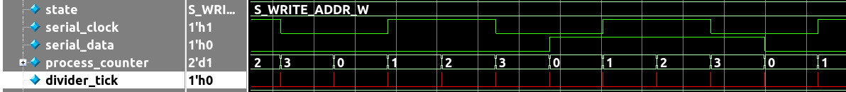
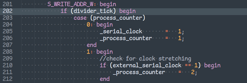
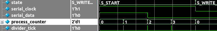
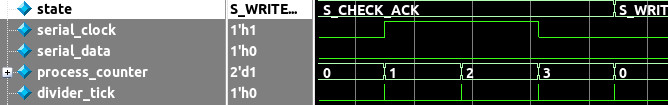
As seen in the Figure 5, each time our divider tick pulses process counter is incremented (the state executes a process). This is because each state is partitioned into 4 processes (process_counter = 0, 1, 2, 3). SCL is toggled during the middle two processes ( 1 and 2 ). SDA bit data is asserted during process_counter = 0. This allows for a quarter SCL period of setup time

Clock Stretching
When process_counter = 1, the SCL line is released and placed in the high Z state. During this time the master checks for any clock stretching being attempted by the slave. If no clock stretching is detected, the master will iterate through the remaining processes and continue as normal. However if clock stretching is detected, the master will stay in the process_counter = 1 process until SCL line is high once more.
If clock stretching is enabled, it is recommed to also enable the "cycle timer".
Detailed State Machine Flow
Below we will go through each state the state machine cycles through for a Read and then a Write operation.
Read Operation
1. S_IDLE (8’h00)
Save the following inputs into registers: device_address (spi slave device address), register_address (spi slave target addr), mosi_data (spi slave data to write), read_write (read/write status bit). SDA and SCL are parked high in this state.
If enable state is high, we move to the S_START state
2. S_START (8’h01)
Here we execute the I2C start sequence by setting SDA low, followed by SCL low.
3. S_WRITE_ADDR_W (8’h02)
The device address Is sent with a 0 appended to the LSB to signify a write operation. Although the end goal is to read a i2c address we must first write the I2C address value we want to read from to the I2C slave. Most significant bit is transmitted first.
4. S_CHECK ACK (8’h03)
Checks for the ACK bit response from salve. A low bit from the slave will signify a ACK. If a NACK bit is sent instead (high bit) the state machine will return to IDLE. The “last_acknowledge” register is set high if ACK is received and low if a NACK bit is received. This can be used as an error flag.
5. S_WRITE_REG_ADDR (8’h04)
Writes the address of the register to be read one bit at a time. Most significant bit is transmitted first. If the address consideres of more than one byte, a acknowledge check is done after each byte before transmitting more bits.
6. S_CHECK_ACK (8’h03)
Checks for the ACK bit response from salve. A low bit from the slave will signify a ACK. If a NACK bit is sent instead (high bit) the state machine will return to IDLE. The “last_acknowledge” register is set high if ACK is received and low if a NACK bit is received. This can be used as an error flag.
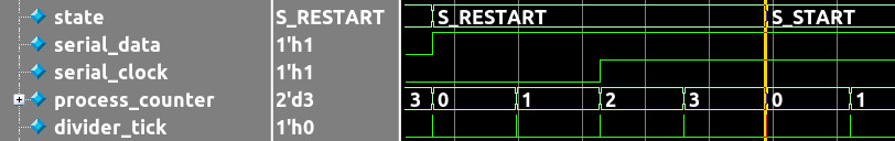
7. S_RESTART (8’h05)
Send Restart sequence. SDA High followed by SCL High.
8. S_WRITE_ADDR_R (8’h06)
The device address Is sent with a 1 appended to the LSB to signify a read operation.
9. S_CHECK_ACK (8’h03)
Checks for the ACK bit response from salve. A low bit from the slave will signify a ACK. If a NACK bit is sent instead (high bit) the state machine will return to IDLE. The “last_acknowledge” register is set high if ACK is received and low if a NACK bit is received. This can be used as an error flag.
10. S_READ_REG (8’h07)
The register is finally read and stored into the "miso_data" output register. Data is shifted in most significant bit first. The master will send an ACK bit after each byte it reads. If multiple bytes are read from the slave, the master will read the successive byte after sending the ACK bit.
11. S_SEND_ACK (8’h0E)
Sends an ACK bit (low bit). This is done when reading 16 bit data. The most significant byte is read, then this ACK bit is sent by the master which tells the slave to continue with the least significant byte of data.
12. S_SEND_NACK (8’h08)
Sends a NACK bit (high). This is done when all reading is completed. Sending a ACK bit instead at point will allow for burst reading if the slave supports it.
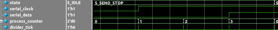
13. S_SEND_STOP (8’h09)
Sends the stop sequence to end the I2C transaction. The stop sequence is done by setting SCL high followed by SDA high.
Write Operation
1. S_IDLE (8’h00)
Save the following inputs into registers: device_address (spi slave device address), register_address (spi slave target addr), mosi_data (spi slave data to write), read_write (read/write status bit). SDA and SCL are parked high in this state.
2. S_START (8’h01)
Here we execute the I2C start sequence by setting SDA low, followed by SCL low.
3. S_WRITE_ADDR_W (8’h02)
The device address Is sent with a 0 appended to the LSB to signify a write operation. Although the end goal is to read an address we must first write the address value we want to read from to the slave.
4. S_CHECK ACK (8’h03)
Checks for the ACK bit response from salve. A low bit from the slave will signify a ACK. If a NACK bit is sent instead (high bit) the state machine will return to IDLE. The “last_acknowledge” register is set high if ACK is received and low if a NACK bit is received. This can be used as an error flag.
5. S_WRITE_REG_ADDR (8’h04)
Writes the address of the register to be written to one bit at a time. Most significant bit is transmitted first. If the address consideres of more than one byte, a acknowledge check is done after each byte before transmitting more bits.
6. S_CHECK ACK (8'h03)
Checks for the ACK bit response from salve. A low bit from the slave will signify a ACK. If a NACK bit is sent instead (high bit) the state machine will return to IDLE. The “last_acknowledge” register is set high if ACK is received and low if a NACK bit is received. This can be used as an error flag.
7. S_WRITE_REG_DATA (8'h0A)
Writes the data to the target register one bit at a time. Most significant bit is transmitted first. A check for ACK and occurs after a byte is sent. If more than one byte of data is to be sent, the following byte will be transmitted after each successful ACK check.
8. S_CHECK ACK (8'h03)
Checks for the ACK bit response from salve. A low bit from the slave will signify a ACK. If a NACK bit is sent instead (high bit) the state machine will return to S_IDLE. The “ack_recieved” register is set high if ACK is received and low if a NACK bit is received. This can be used as an error flag.
9. S_SEND_STOP (8'h09)
Sends the stop sequence to end the I2C transaction.
Recommended Usage
When using this master the "busy" output is a cirtical flag to monitor in order to easily keep track of what the master is doing. It is recommend to first set the configuration inputs of the master. This includes "read_write", "register_address", "mosi", "device_address", and "divider". Then query the "busy" signal, once it is low set "enable" high. Once "busy" output goes high, we set "enable" low. Finally once "busy" is low again, we know the transaction has been completed. If a read operation was requested, the read word will be available via the "miso_data" output.
If clock stretching is enabled, it is recommed to also enable the "cycle timer". To enable this time out timer set the CLOCK_STRETCHING_MAX_COUNT parameter to a non zero value. When this is done the master will wait that many divider tick pulses before timing out during clock stretching. By not using this feature, the master can get stuck in the clock stretching check phase of its operation if a slave starts misbehaving. This max count value can also be used to limit the amount of clock stretching any slave can request. This can be important to do if the timing of operations is critical in a system that is using this I2C master module. A brief overview of the "cycle_timer" module can be found below.
Cycle Timer Overview
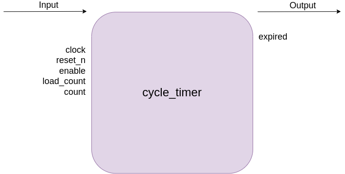
| Name | Type | Width | Direction | Description |
|---|---|---|---|---|
| clock | wire | 1 | input | Main system clock |
| reset_n | wire | 1 | input | Active low reset |
| enable | wire | 1 | input | Active high enable signal that will let the timer run. |
| load_count | wire | 1 | input | Active high signal that will set the counter value to the value supplied at the "count" input port. |
| count | wire | BIT_WIDTH | input | Value the counter will be set to when the "load_count" input is high. |
| expired | logic | 1 | output | Active high flag indicating the timer has popped. Occurs when the counter decrements down to zero. |
| Name | Description |
|---|---|
| BIT_WIDTH | Number of bits the counter register should be. This effectively sets the max value of the counter. |