Circuit to Convert K-LINE (ISO 9141-2 and ISO 14230-4) to Full Duplex UART
What Is K-Line?
In the 90s to early 2000s K-Line was the de facto way of communicating to vehicle ECUs through the OBD2 port. Today almost all vehicles have moved on to CAN interfaces, but millions of vehicles remain on the road today that use K-Line. K-Line as defined by the ISO 9141-2 and ISO/DIS 14230-4 standard can simply be reduced to a single wire bidirectional half duplex UART interface.
The Circuit
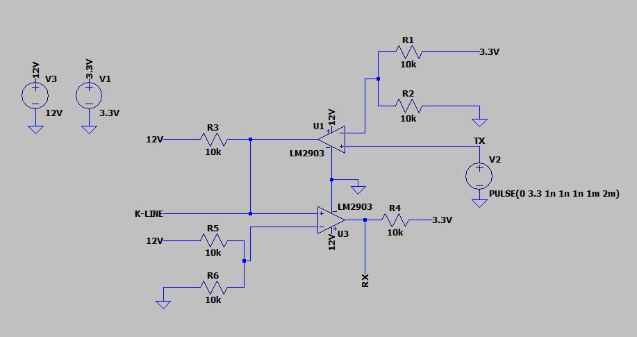
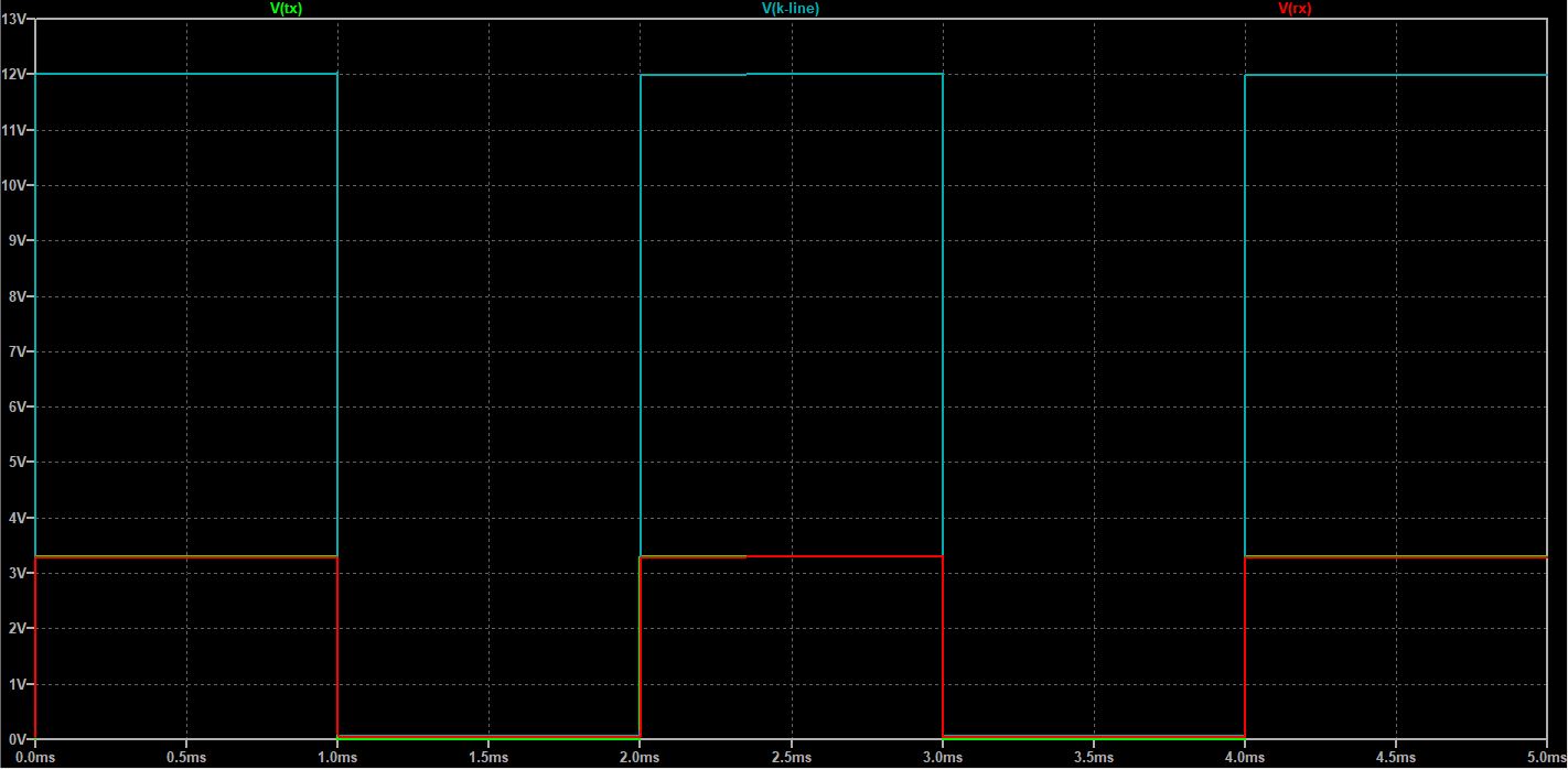
To interface with this standard using a full duplex UART system found on basically all MCUs we can create a simple circuit using two comparators and some resistors. This circuit also does logic level conversion from the standard 3.3V/5V that most microcontrollers use to the 12V logic level found on K-LINE systems. As shown in Figure 1 our TX signal from the MCU is fed into the non-inverting input of opamp U1. Once the voltage of the TX signal is less than the voltage at the non-inverting input of U1 (3.3/2 volts) our comparator U1 will output low. Otherwise the output is pulled up high to 12V via our pullup resistor R3. This scheme allows us to transmit data from the MCUs TX output to the K-LINE input. Data being transmitted from the K-LINE will also be outputted to the RX of the MCU via the mechanics except this time comparator U3 will be doing the work. A simulation plot of this circuit in action can be observed in Figure 2
As seen in Figure 2, any TX signal being fed into this circuit will be echoed back out the RX line. This allows for sanity checks in your microcontroller firmware, but it also means your RX buffer will contain the data you just transmitted. Therefore, it is important to distinguish between echoed back TX data vs actual RX data from the K-LINE.
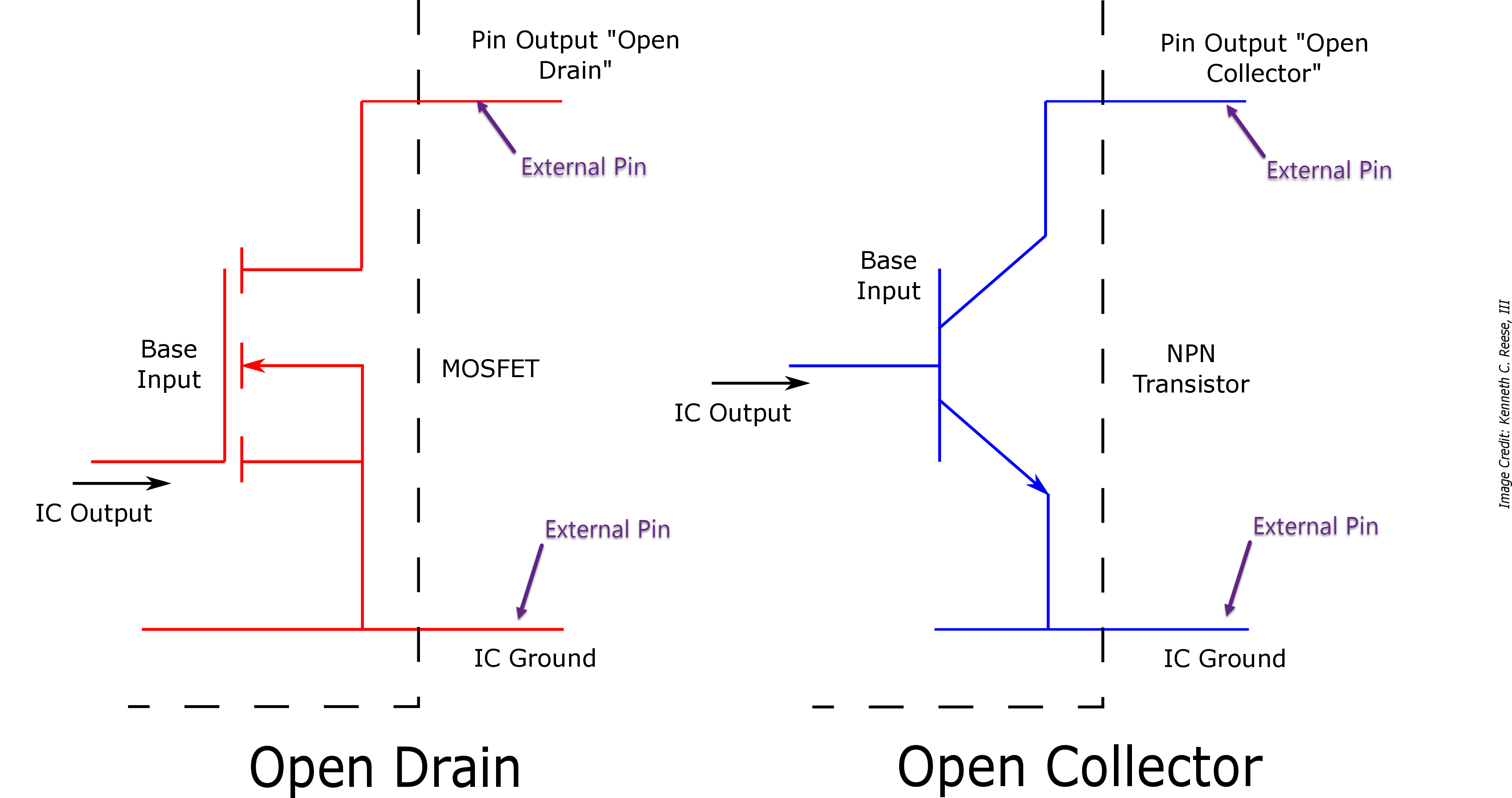
Lastly, it’s important to note that comparators such as the LM2903 have open drain or open collector outputs. This means the op amp cannot drive the output high. As shown by Figure 3, the op amps output is fed into the base/gate of a transistor who has its collector/emitter open. The output of the op amp chip is this open node. What this means is that the output of these comparators MUST be pulled up for proper operation.