Temperature Compensated Analog Voltage to Frequency Converter Circuit
Implementing a voltage to frequency converting system is a trivial task in the digital realm using things like microcontrollers but it’s a fun engineering exercise to do it using only analog components.
In order to achieve different frequencies using a varying voltage we need a component that relates time and voltage. The best component that can achieve this is the capacitor. The charging current of a capacitor is \( i(t) = C* \frac {dV}{dt}\). We can re work this equation as \( V(t) = \frac{1}{C*i*t}\). This gets us close but the problem is our voltage still depends on a time varying current. However if the current was constant we would have \( V(t) = \frac{1}{C*i*t}\) which gives us a voltage that is directly a function of time.
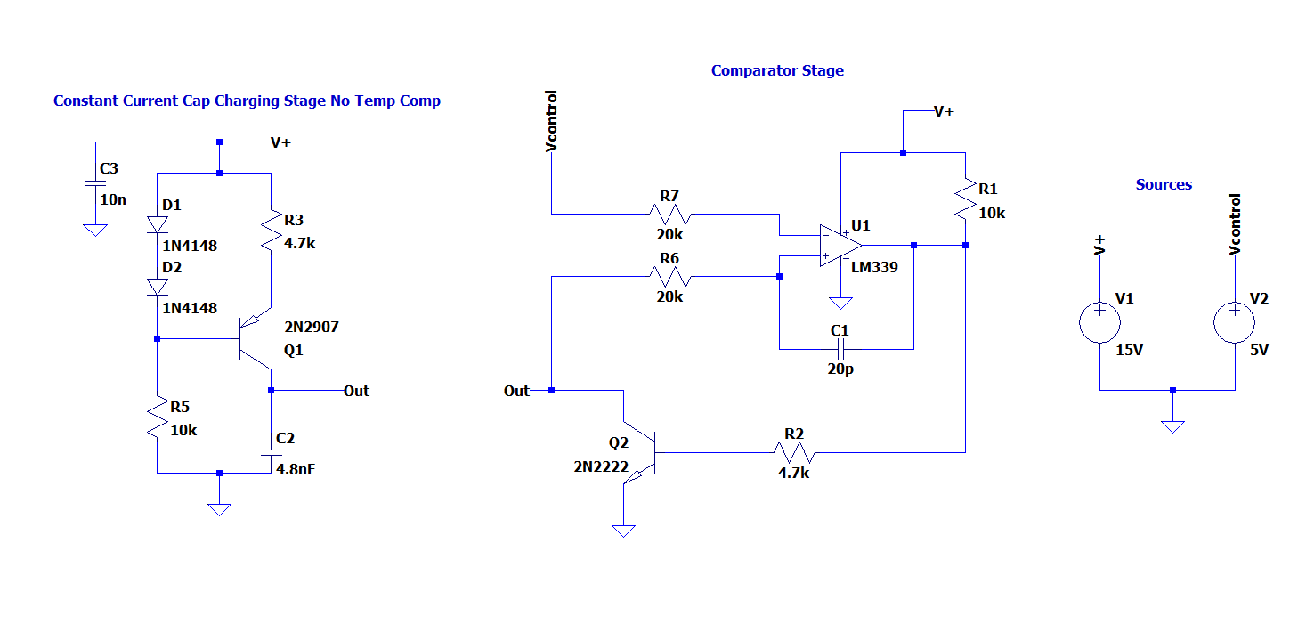
In order to have such a current source we need to build a constant current source by biasing a single PNP transistor and connecting the capacitor as the load (shown below).
The base voltage of Q1 can be calculated as \(V_{B} = V_{+} - 2*V_{D}\) where \(V_{D}\) is the forward voltage drop of D1 and D2. Assuming Q1 is active, \(V_{E} = V_{B} + V_{BE}\) where \(V_{BE}\) is the base to emitter voltage of Q1. Therefore our constant current is defined by \(I_{C} = \frac{V_{+} - V_{E}}{R3}\).
The collector of Q1 is connected to the non inverting input of a comparator and a controllable voltage source, \(V_{control}\), to the inverting input of a comparator. When the voltage on the capacitor is greater than \(V_{control}\), the output of the comparator is high and the opposite is true when the capacitor voltage is less than \(V_{control}\).
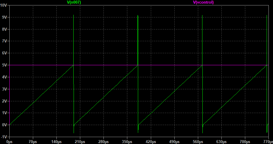
When the comparator output is high, Q2 is biased ON and the capacitor is discharged. This repeats creating a sawtooth capacitor voltage whose frequency is inversely proportional to the input voltage \(V_{control}\). By extension the frequency of the comparator’s output is the same and also inversely proportional to \(V_{control}\).
Details:
- The maximum value of \(V_{control}\) must be such that it keeps Q1 out of saturation. Increasing \(V_{control}\) will increase the collector voltage of Q1. The collector to emitter voltage must be greater than the diode voltage of the BJT in order for the transistor to remain in the linear active region.
- The minimum value of \(V_{control}\) will depend on C1. If the \(V_{control}\) is too low, C1 will not have enough time to discharge. Normally this is not a problem however since the discharge of a capacitor is exponential, the lower the voltage it has to discharge to, the more time is required. Therefore at some point if \(V_{control}\) is too low, the frequency will start to decrease as \(V_{control}\) is decreased.
- The op amps input resistors R6 and R7 are used to minimize offset voltages caused by the bias currents that flow into the inputs.
- R1 is used as a pull up resistor for the comparators output. Since the LM339 has an open collector output it can only sink current. Therefore we need the pull up resistor to bias Q2.
- C1 is critical for the operation of this circuit. Without it, our capacitor C2 will not have enough time to discharge. By placing C1 between the output and non inverting input we add some much needed hysteresis to the comparator. The high frequency rising edge of the comparators output shorts through C1 which creates a voltage spike at the non inverting input. This makes the output of the comparator stay high longer, ensuring the capacitor C2 fully discharges. The resistor R6 isolates C2 from the voltage spike.
Adding Temperature Compensation:
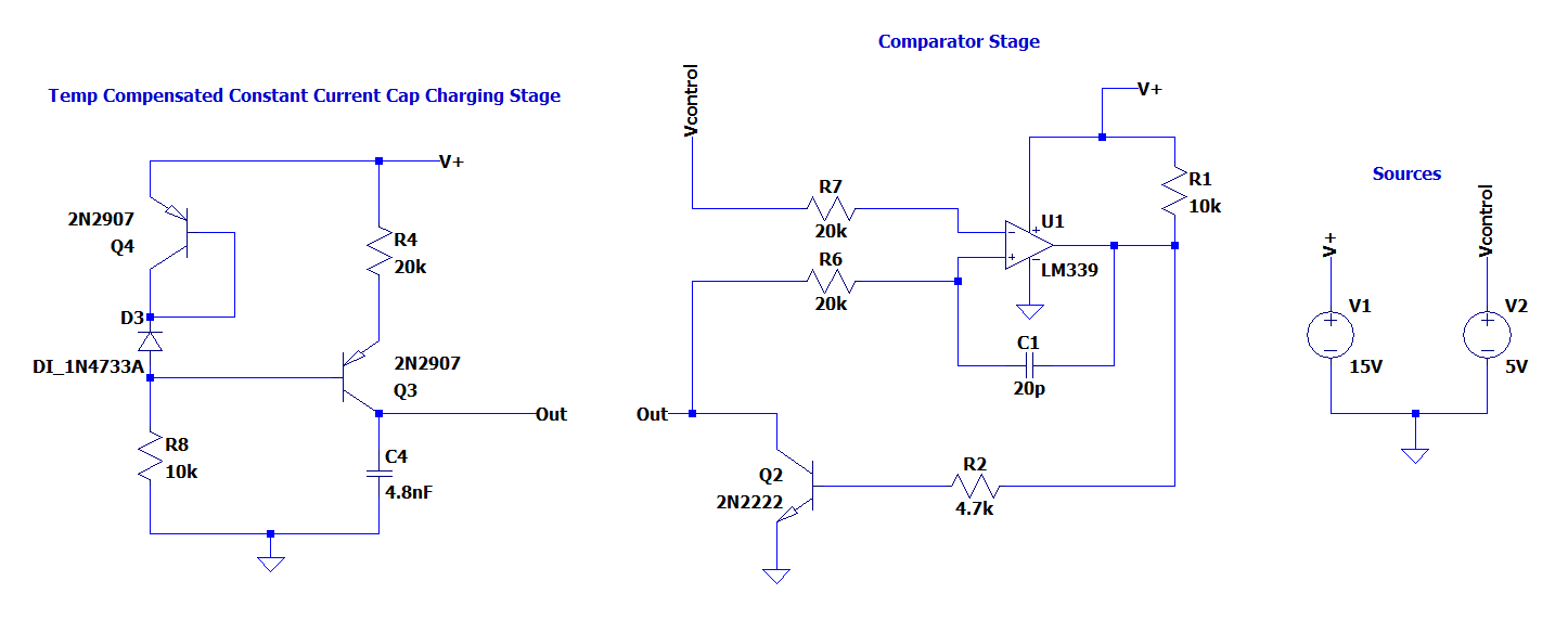
The problem with the original circuit is that our constant current can significantly vary across different temperatures. This is because the base to emitter voltage of the current sources transistor varies with temperature. In order to combat this we need a new circuit that compensates for these changes such as the one below.
The circuit above implements a constant current source that does not depend on the base emitter voltages of the transistors. We can prove this with the following calculations.
The base voltage of Q3, \(V_{B3}\), is calculated to be \(V_{+} - V_{EB4} - V_{Z}\) (\(V_{Z}\) is the zener voltage of D3). The important note here is \(V_{EB4}\) changes in temperature which will in effect change \(V_{B3}\). (\(V_{Z}\) will also change with temperature but zener voltages change relatively very little with respect to temperature ( as low as 0.005%/C).
By knowing \(V_{B3}\) we can calculate \(V_{E3}\) to be \(V_{B3} - V_{BE3}\) . Therefore \(V_{E3} = V_{+} - V_{EB4} - V_{Z} - V_{BE3}\). Because Q3 and Q4 are identical transistors (ideally they should be a matched pair on the same piece of silicone) the \(V_{BE3}\) and \(V_{EB4}\) components of the equation will cancel out leaving us with \(V_{E3} = V_{+} - V_{Z}\). With that we can calculate the temperature indifferent emitter current of Q4 as \(I_{E 4} = \frac{V_{Z}} {R4}\).
Quantifying the Results of Temp Compensation
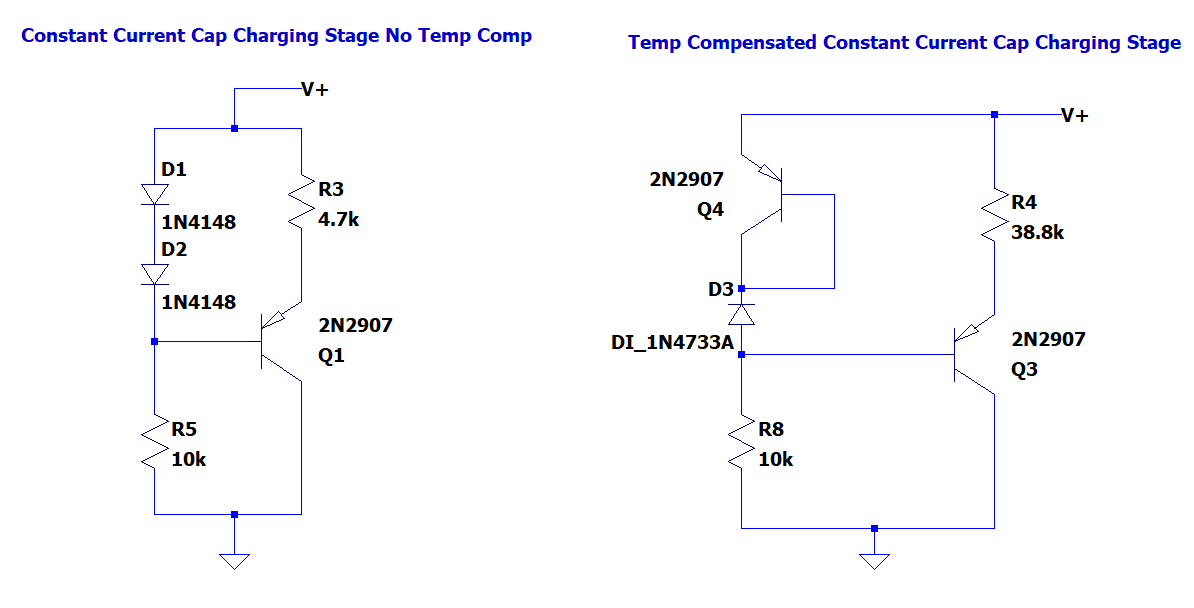
To prove the effectiveness of the temperature compensation, we can simulate the compensated and non compensated circuit and sweep the temperature. Both of the current sources shown below are designed for a constant current of 127uA. A temperature of 0C and 150C was used. As we can see below the difference is huge. There is only 0.58% difference between the compensated currents and a 53.65% difference between the non compensated currents.
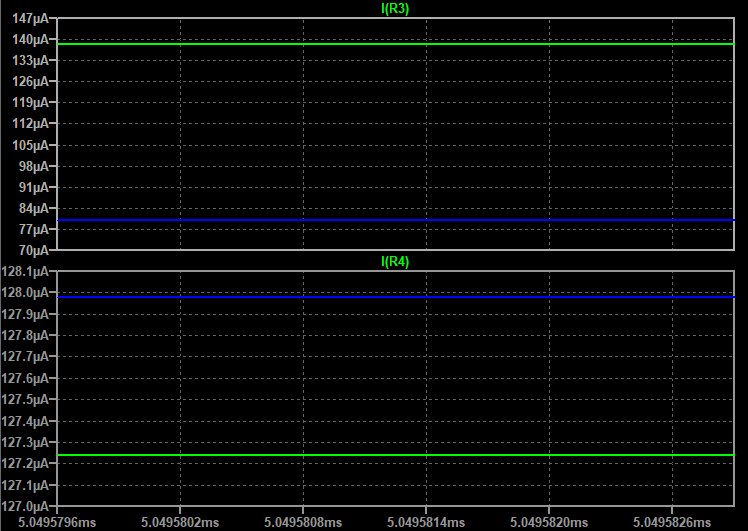
Bottom: With Compensation
| Temperature | No Compensation | With Compensation |
|---|---|---|
| 0 C | 138.337 uA | 127.238uA |
| 150 C | 79.820 uA |
127.976 uA |
Choosing the Ideal Capacitor:
To make this circuit behave as consistently as possible we need a capacitor that is very stable. This means the capacitance must not change with temperature and it must be resilient to physical effects such as vibrations.
Ideal choices:
NPO
Mica
Tantalum
Passable:
Polystyrene (capacitance can permanently change with high temperatures such as when being soldered)
Not Ideal:
The following capacitors are generally more sensitive to temperature and should be avoided if possible. The ceramic capacitors also exhibit noise under vibrations via the piezoelectric effect. This may not change behavior of the circuit and should be kept in mind.
Mylar
Electrolytic
Ceramic (X5R, X7R, Y5V, Z5U)\
Building and Characterizing the Circuit:
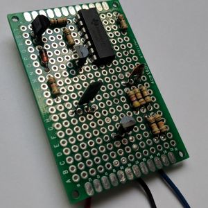
The circuit was built and behaved as simulated, exhibiting the results shown in the table below.
| Control Voltage | 10 | 9.5 | 9 | 8.5 | 8 | 7.5 | 7 | 6.5 | 6 | 5.5 | 5 | 4.5 | 4 | 3.5 | 3 | 2.5 | 2 | 1.5 | 1 | 0.5 |
|---|---|---|---|---|---|---|---|---|---|---|---|---|---|---|---|---|---|---|---|---|
| Output [kHz] | 5.15 | 5.43 | 5.75 | 6.1 | 6.45 | 6.85 | 7.35 | 7.94 | 8.55 | 9.26 | 10.2 | 11.2 | 12.6 | 14.4 | 16.6 | 19.6 | 24 | 31 | 43.1 | 70.4 |
$$f_{out} = 42.711V^{-0.9}$$

