
Dickson Charge Pump
The Dickson Voltage Multiplier is a useful and cost-effective circuit that can be used to create higher voltages when designing a system that is powered by a low voltage source such as a battery. Putting the circuit together is easy however understanding how it works can be a bit tricky. Furthermore, it’s essential to have a good understanding of how it works to troubleshoot and size components in your design.
General Overview and Theory:
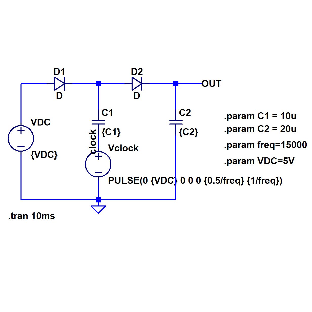
Figure 1: single stage Dickson Votlage Multiplier
\(V_{DC} = \ DC\ voltage\ source\)
\(V_{clock} = \ Square\ wave\ clock\ signal\)
\(V_{D} = \ Forward\ bias\ voltage\ of\ diode\)
A single stage Dickson Voltage Multiplier effectively has two states of operation depending on the value of Vclock.
Let’s assume we just powered on our circuit and Vclock starts low.
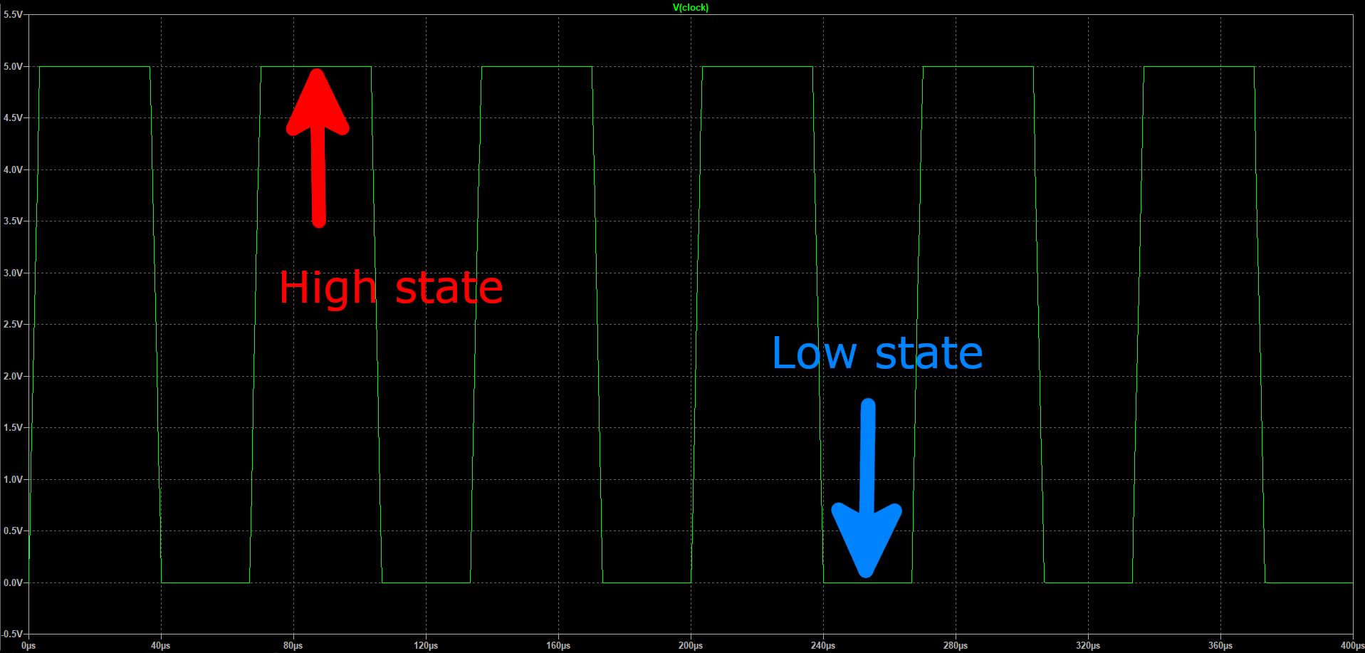
State 1: Vclock is low
When Vclock is low, the voltage across \(C_1\) and the voltage at node A is \(V_{DC}\ – V_D\). Also, the voltage across \(C_2\) is \(V_{DC} – 2*V_D\).
State 2: Vclock is high
Now that the clock is high, node A will be pushed to \(V_{clock} + V_{DC} – V_D\). As soon as this occurs we enter a situation where the voltage at node A is higher than the Vdc and node B.
Before we go forward, lets switch to a more first principles oriented approach by focusing explicitly on where charge is stored and transferred. The amount of charge stored in \(C_1\) is \(Q_{C1} = C_1 * (V_{DC} -V_D)\). Because of the strategic placement of our diodes, and because the voltage at node A is higher than node B, charge will be pumped from \(C_1\) to \(C_2\) until we reach an equilibrium state where the voltage at node B is equal to the voltage at node A minus VD. This occurs because as charge goes out of \(C_1\) and into \(C_2\), the voltage across \(C_1\) decreases ( \(V = Q/C\) ) while the voltage across \(C_2\) increases. We can define the amount of charge that gets transferred as \( \Delta Q\) and use Kirchhoff’s Voltage Law to calculate \( \Delta Q\):
$$V_{clock} + \frac{Q_1 - \Delta Q}{C_1} - V_D = \frac {Q_2 + \Delta Q}{C_2}$$
$$\frac{\Delta Q}{Q_2} + \frac{\Delta Q}{C_1} = (V_{clock} + \frac{Q1}{C1} - {V_D} - \frac{Q_2}{C_2} ) $$
$$\Delta Q = ( V_{clock} + \frac{Q1}{C_1} - V_D - \frac{Q_2}{C_2} ) / ( \frac{1}{C_1} + \frac{1}{C_2}) $$
Example:
\(C_1\)= 1uC
\(C_2\) = 10uC
\(V_{DC}\) = 16V
\(V_{Diode}\) = 0.7V
\(V_{clock}\) = 0-16V
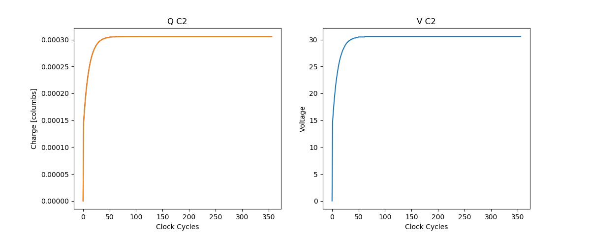
Using the equations from the previos section we can calculate the amount of charge stored in C2 each cycle and thus the voltage. Assuming this is the very first cycle of the clock, the amount of charge initially stored in \(C_2\) is \(Q_{2initial} = C_2* (V_{DC}-2*V_D)\). Therefore we can calculate a \(\Delta Q\) of 14.54 uC being pumped into \(C_2\) which will bump up the voltage at node A to 14.6V. This process will repeat for each cycle of the clock until the charge in \(C_2\) is equal 306uC. to and by extension until the voltage across \(C_2\) is equal to 30.6V. By doing these calculations we can see it takes about 60 cycles for the output to reach its final voltage. Ofrourse this assumes there is no load and that all the components are ideal. The Python code used to calculate these results is posted below. A LTSpice simulation file is also available at the very end of the article.
| Cycle | \(Q_{C2}\) | \(V_{C2}\) |
|---|---|---|
| 1 | 0.000146 | 14.6 |
| 2 | 0.00016 | 16.1 |
| 3 | 0.000174 | 17.4 |
| 4 | 0.000186 | 18.6 |
| 5 | 0.000197 | 19.7 |
| 6 | 0.000207 | 20.7 |
| 7 | 0.000216 | 21.6 |
| 8 | 0.000224 | 22.4 |
| … | … | … |
| 62 | 0.000306 | 30.6 |
import numpy as np
import matplotlib.pyplot as plt
c1 = 1E-6
c2 = 10E-6
vDC = 16
vD = 0.7
vclk = 16
qC1 = c1*(vDC-vD)
qC2init = c2*(vDC-2*vD)
qC2final = c2*(vDC-2*vD+vclk)

qC2 = []
qC2.append(0)
qC2.append(qC2init)

while(qC2[-1] != qC2final):
    dQ = (vclk + qC1/c1 - vD - qC2[-1]/c2)/( 1/c2 + 1/c1)
    qC2new = qC2[-1] + dQ
    if(qC2new == qC2[-1]):
        break
    qC2.append(qC2new)

qC2 = np.array(qC2)
plt.subplot(1, 2, 1)
plt.plot(qC2)
plt.ylabel('Charge [columbs]')
plt.xlabel('Clock Cycles')
plt.title('Q C2')
plt.subplot(1, 2, 2)
plt.plot(vC2)
vC2 = qC2/c2
plt.ylabel('Voltage')
plt.xlabel('Clock Cycles')
plt.title('V C2')
qC2 = np.round(qC2, 6)
vC2 = np.round(vC2, 1)
Optimizing Design:
\(C_1\):
Choosing the size of \(C_1\) is dependent on the amount of power the load we are driving requires. This is because when we are driving a load, the charge that \(C_1\) is able to pump into \(C_2\) must at the very least be equal to the amount of charge the load requires. If that requirement is not met, charge will be depleted from \(C_2\) and therefore we will have too much ripple and/or severe voltage drags. In other words we need to make sure the average power \(C_1\) is able to deliver is more than the average power our load requires. To calculate the average power \(C_1\) can deliver, we first calculate the energy stored \(C_1\), \(E = 0.5CV^2\) Joules. To calculate the average power we multiply by \(2*f_{clock}\) since our clock is running at 50% duty cycle.
\(C_2\):
The impedance of any Capacitors is defined by \(X_c = 0.5\pi fC\) so we can drive down the impedance of \(C_2\) by increasing the capacitance and therefore increasing our efficiency. A large \(C_2\) will also mean less voltage ripple since we will have a greater “bucket” of charge that the load can draw from. We can define the amount our voltage will ripple as \(\Delta V = \frac{\Delta Q}{C_2}\) where \(\Delta Q_C\) is the amount of charge that the load draws from \(C_2\). Therefore the larger \(C_2\) is the smaller our voltage ripple, \(\Delta V\), will be. However, the larger \(C_2\) is, the longer it will take to fully charge. This means our output voltage will take longer to reach its final voltage. So for designs that need a quick response from the off state should consider not making \(C_2\) too large. Last but not least, Because the sizing requirements of \(C_2\) is generally lax, it is a good component to manipulate in order to tune the output impedance of the multiplier for designs that require specific impedances.
Series Resistance:
Since we’re always working with non ideal components in real life, choosing capacitors with the lowest series resistance possible is import to minimize the amount of power that gets lost and to ensure our capacitors get charged as quickly as possible to minimize charging losses. Series resistance can also always be lowered by placing capacitors in parallel.
Diodes:
For maximum efficiency we need diodes with the lowest forward bias voltage and with the lowest on resistance. Generally Schottky diodes work best.
Clock Frequency:
As previously stated, the impedance of a capacitor is defined by Xc = 1/2pifC and the average power C1 will deliver is fCV^2. Therefore the higher our clock frequency the better the efficiency of our design will be. However if we go too high, the parasitic inductance of our capacitors will actually cause the impedance of our components to increase. At what frequency this occurs depends on the type of capacitors used. Furthermore, the parasitic inductance can be lowered like the series resistance by placing capacitors in parallel.