SPWM Variable Frequency Single Stage Inverter Design
Overview
SPWM is a PWM technique used to create a wave of pules that average out to a sine wave. One advantage of creating sine waves with this technique is being able to change wave’s frequency on demand. This is particularly useful when used to drive synchronous machines as it enables us to dynamically change the speed of the machine. In the following post we discuss the implementation of a single phase, single state, SPWM inverter. Although this particular design is a low power implementation, a high power version can easily be created by switching to more suited components such as IGBTs.
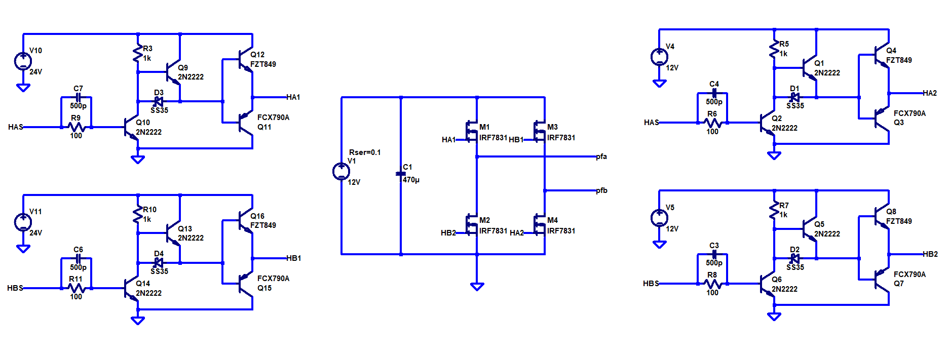
Like any single phase and single stage inverter, we require the use of 4 switches in a H bridge configuration. More stages can be achieved by cascading bridges but for this design we will only use a single stage. The magic of the SPWM inverter all boils down to the control signals which drive the switches (mosfets in this example).
SPWM Control
The SPWM control signal is created using two triangle carrier waves and a reference sine wave. The frequency of the outputted SPWM sine wave will be the same as the reference sine wave. Increasing the frequency of the carrier waves will result in higher density pulses which ultimately create a more accurate SPWM sine wave.
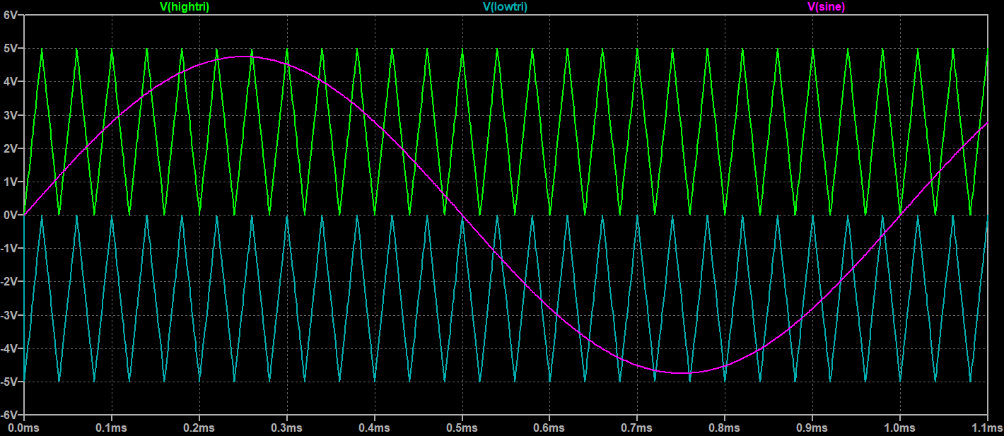
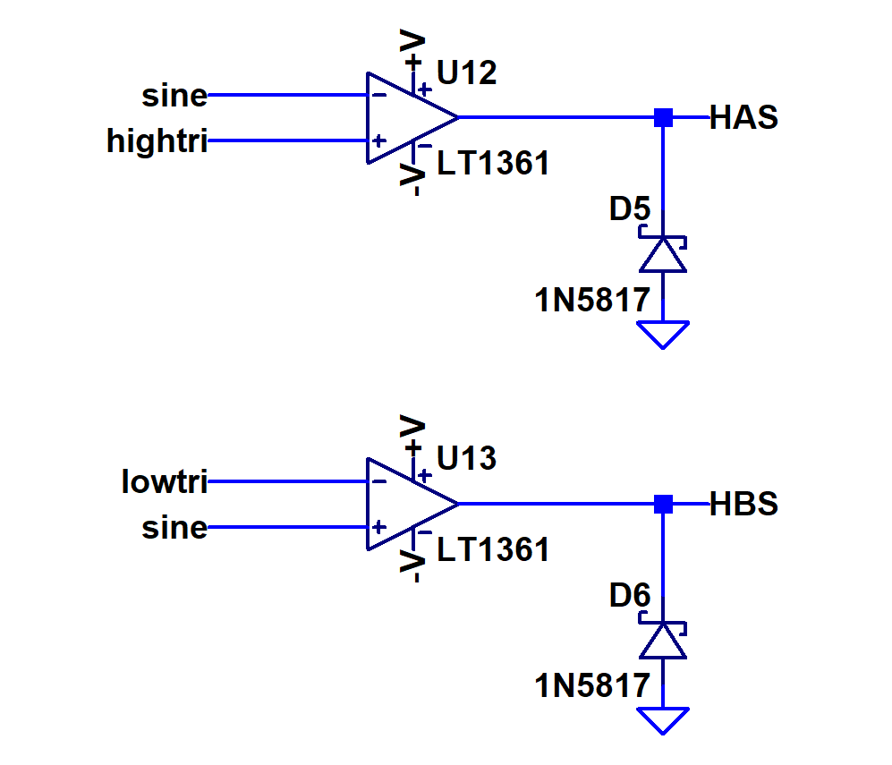
As seen by the Figure-1, the upper wave goes from 0 to 5V and the bottom wave goes from 0 to -5V. The amplitude of the reference sine wave is 4.75, slightly less that of the carrier waves. This is done to avoid a situation where the amplitude of carrier wave is equal to the sine wave. Furthermore, it is important for the carrier waves to be in phase because we don't want a situation where the top carrier, bottom carrier, and sine wave all are equal to zero volts. A situation like that can cause a shoot through condition in the bridge. By feeding these waves into two comparators, as shown in Figure-2, we obtain our control signals HAS and HBS. These are then delivered to the gate drivers which drive the mosfets (Figure-3). The comparators shown in Figure-2 produce the following logic:
hightri < sine: HAS is HIGH
hightri > sine: HAS is LOW
lowtri > sine: HBS is LOW
lowtri < sine: HBS is HIGH
Triangle Carrier Wave Generator
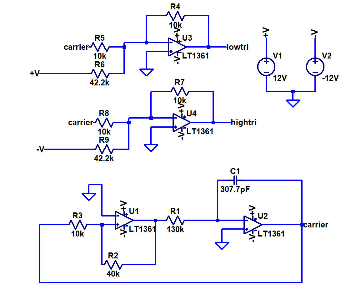
The triangle wave is generated using an oscillator made from a non-inverting smith trigger whose output is fed into an inverting integrator. We choose the switching voltage, Vs, of the smith trigger with R3 and R2. Vs = +V*(R3/R2). This means when Va>Vs Vb= +V. When Va < Vs, Vb = V-.
The integrator's transfer function can be solved via KCL and is found to be -Vb/R1 = C*(dVcarrier/dt). Therefore dVcarrier/dt = -Vb/(RC). This means that if Vb is positive, the output voltage Vcarrier will decrease at a rate of -Vb/(RC) per second and vice versa.
Since Vb is the output of our smith trigger, we know Vb will either be +V or -V. Let’s assume the circuit starts with Vb being +V and Vcarrier being 0V. At this point, Vcarrier will begin to decrease at a rate of -Vb/RC. Vcarrier will eventually reach the voltage of -Vs after (RC*Vs)/Vb seconds. Since Vcarrier is fed back in as the input to our smith trigger, the trigger will switch its output (Vb) to -Vs because the input is now lower than switching voltage Vs. Now that Vb is negative, the output of the integrator, Vcarrier, will ramp up from -Vs to Vs which will take a total of 2*(RC*Vs)/Vb seconds. At this point our trigger will once again swing its output voltage Vb to +Vs. Now just like before, Vcarrier will go back down at a rate of -Vb/(RC*Vs) seconds. After (RC*Vs)/-Vb seconds, Vcarrier carrier will have a voltage of zero meaning we completed one whole period. By extension, the total period of our triangle carrier wave is 4*(RC*Vs)/|Vb| and the frequency is |Vb|/(4*RC*Vs). In order to create a lower and upper carrier wave from this single triangle wave, two summing amplifiers are used.
Sine Reference Wave Generation with a Wien Bridge Oscillator
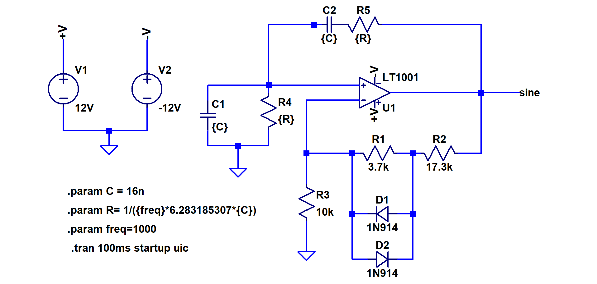
To generate our variable sine wave, a Wien Bridge Oscillator is used. The output of oscillator feeds back to the inverting input through a voltage divider consisting of three resistors, R1, R2, and R3 (let’s ignore the diodes for now). The output also feeds back to the non-inverting input through a ganged series R3 C and parallel R4 C network.
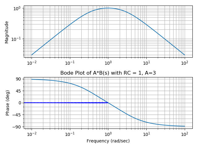
We can consider +V as our input Vin. Since the op amp will drive +V to be equal to -V we can consider -V to be Vin. Therefore Vout/Vin = (R1 + R2 + R3)/R3 meaning the open loop gain, A, is (R1+R2+R3)/R3. The feedback factor B(s) = -V+/Vout which equals -sCR/ sCR + (1+sCR)^2. The bode plot of B(s) reveals that B(s) is a bandpass filter, with a resonant frequency of RC, and a peak gain of 1/3 at the resonant frequency. By choosing an open loop gain (A) slightly greater than 3, we create a system whose loop gain ( A*B(s) ) is greater than 1 at the resonant frequency 1/(2piRC) and less than 1 everywhere else (Figure-6).
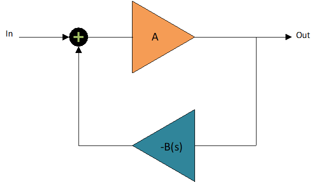
The net result is that noise initially enters as the input, gets amplified by a factor of A, then goes through the feedback B(s) creating a new signal that is dampened everywhere except at the frequency RC. This new signal gets fed back in as the input and the process continuously repeats. Eventually all that’s left is an exponentially increasing sine wave of frequency 1/(2piRC). To stop this sine waves amplitude from increasing past the rail voltage of the op amp, we cap the gain by placing two didoes back to back across R1.
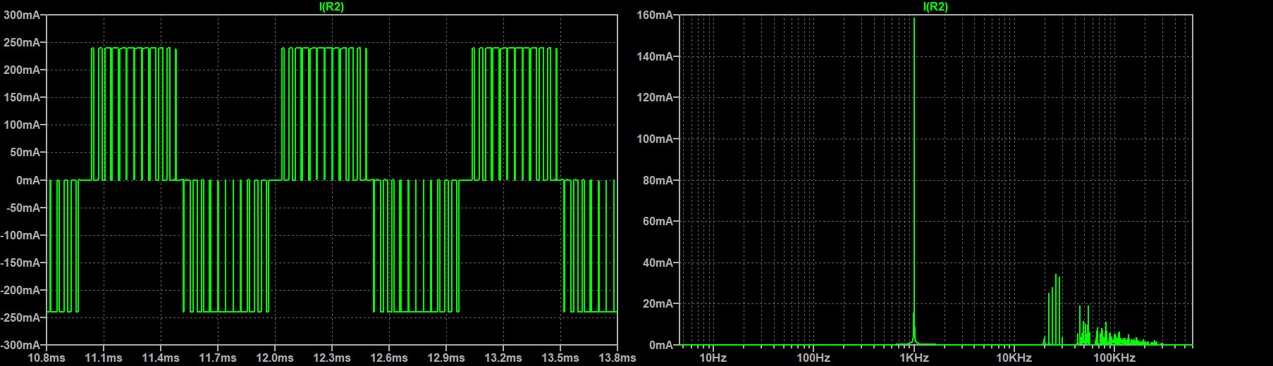
Filtering the Switching Harmonics
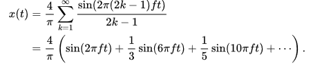
Using PWM square waves to drive the gates injects unwanted harmonics in the output current. The pulsed gates result in pulsed square currents that can be deconstructed via Fourier analysis into a sum of sinusoidal currents at the fundamental frequency (the frequency of the reference control sine wave) and its odd harmonics. Furthermore, the switching frequency (the frequency of the carrier triangle wave) also injects its own harmonics consisting of the fundamental frequency and its odd harmonics just like a square wave.
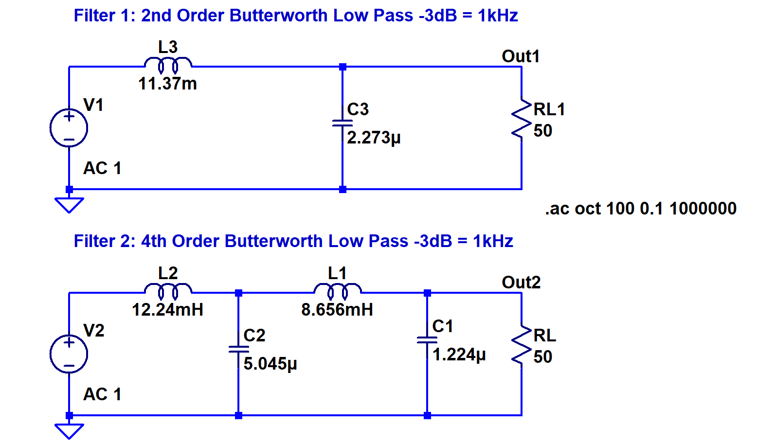
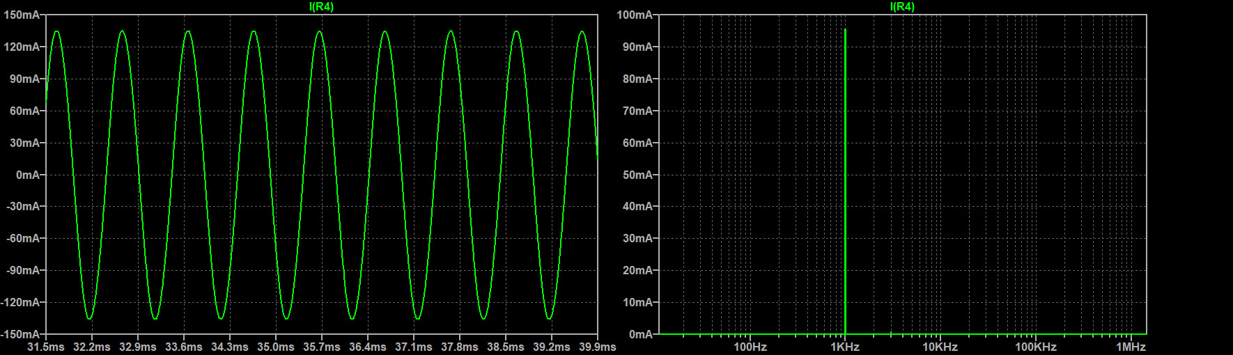
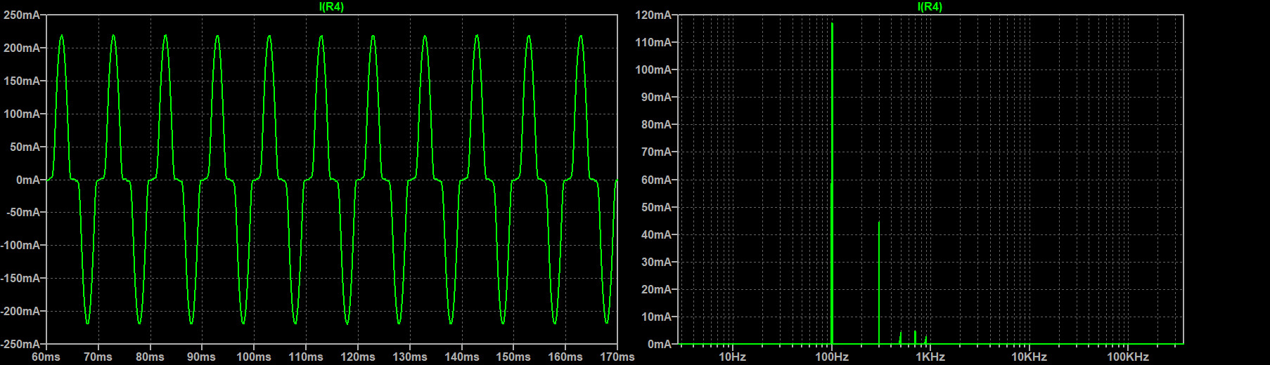
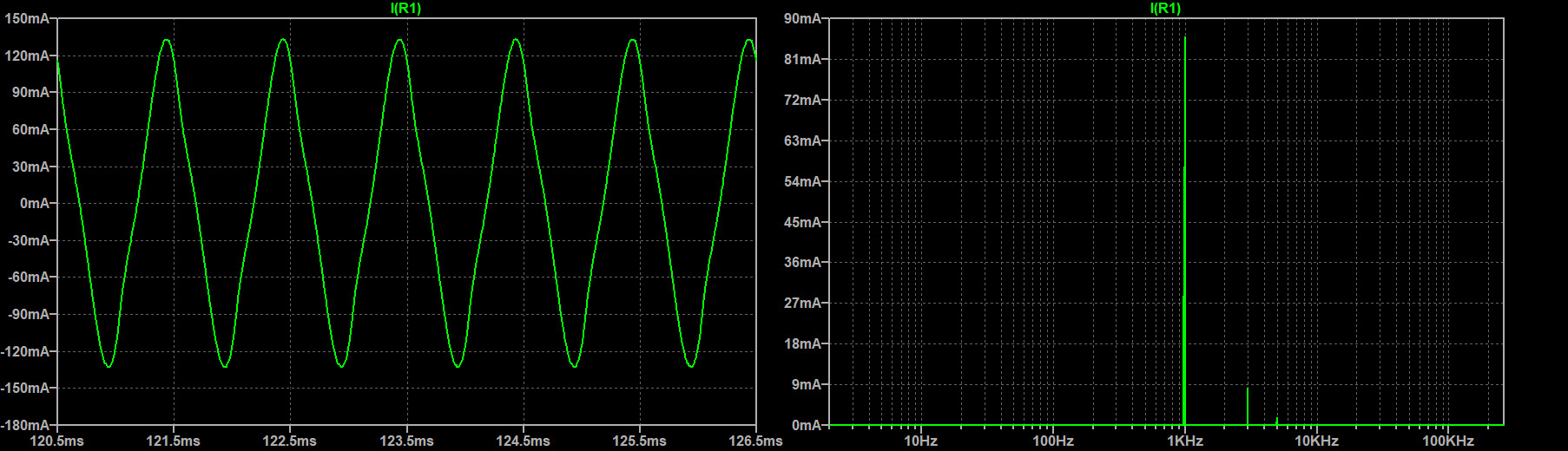
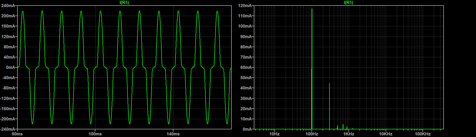
Below we compare the effectiveness of filtering the output using a 2nd order and 4th order passive low pass Butterworth filter with a cutoff frequency of 1kH (Figure-10). Assuming the VFD will operate from 100Hz to 1kHz, this will give us a best-case scenario at 1kHz where all the harmonics will be in the stop band and a worst-case scenario at 100Hz where many of the harmonics will be in the pass band. The switching frequency used is 25kHz. To speed up simulations, an ideal reference wave and carrier wave was used. To measure the effectiveness of the filter, the Total Harmonic Distortion (THD) is calculated.
$$THD\ =\ 100*\frac{ \sqrt{ \sum_{i=0}^n I_{h-i}^2}}{I_f}$$
$$I_{h-i}\ =\ RMS\ Current\ at\ i-th\ Harmonic$$
$$I_f\ =\ RMS\ Current\ at\ Fundamental\ Frequency$$
| THD 1kHz [%] | THD 100Hz [%] | |
|---|---|---|
| No Filter | 55.30266 | |
| Filter 1 | 9.876182 | 38.45812 |
| Filter 2 | 1.417963 | 31.54299 |
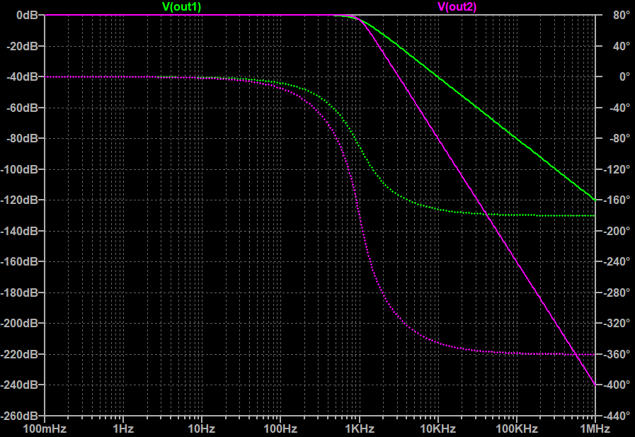
As we can see from the graph above, the results are exactly as expected. Without a filter we have very high THD of about 55% at 1kHz. With the 2nd order filter, the THD drops to 9.9% and the 4th order filter drops it to 1.4%. Unfortunately both filters did not do very well in filtering the 100Hz signal. This is because all the powerful harmonics were still in the pass band. To get a lower THD at these low frequencies, a multi level implementation is needed.
No Filter:
Filter 1 (2nd Order):
Filter 2: (4th Order):